This thread has been locked.

If you have a related question, please click the "Ask a related question" button in the top right corner. The newly created question will be automatically linked to this question.

TPS53513: IV characteristic evaluation between SW and PGND

Part Number: TPS53513


Hi All,

I have a question about TPS53513.

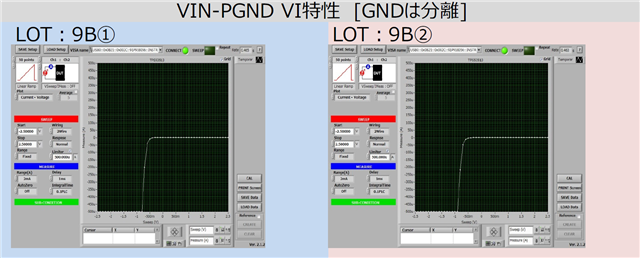
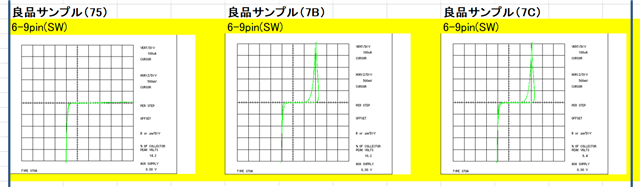
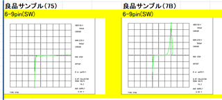
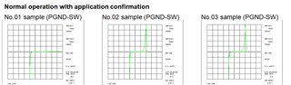
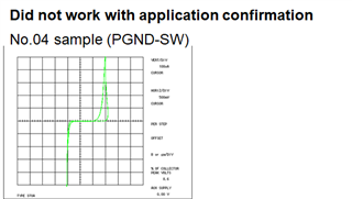
The customer performed an IV evaluation of the SW terminal and the PGND terminal using two samples of good.
The result is as follows.

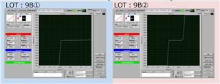
Results will vary depending on the sample.
Why does it result ?

I think there is a mixture of samples in which PGND and GND are internally separated and samples in common.

Best Regards,
Ishiwata

  • Hi Ishiwata,

    Our US team will check it and reply you next Monday.

  • Hi Ishiwata-san,

    Is the curve trace done on the IC alone or connected to other circuitry? Are the parts new, or have they been subjected to some handling? Are the curve traces done by the same method? For example, if PVIN is shorted to PGND, externally or internally, it might cause a characteristic like the one shown. Perhaps they can try curve tracing PGND-PVIN. Is this observation consistent on many units in this lot 9B2, or is it just an observation from a single unit?

  • Hi Ide-san,

    Thank you for your reply.

    Is the curve trace done on the IC alone or connected to other circuitry?
      =>It was done on the evaluation board.
           The customer says that separated PGND and GND on the evaluation board.

    Are the parts new, or have they been subjected to some handling?
      =>It is a good product.

    Are the curve traces done by the same method? For example, if PVIN is shorted to PGND, externally or internally, it might cause a characteristic like the one shown. Perhaps they can try curve tracing PGND-PVIN.
      =>It's done in the same way.
          I'm sorry I couldn't understand. Why would you try PGND-PVIN?

    Is this observation consistent on many units in this lot 9B2, or is it just an observation from a single unit?
      =>It is Only one.

    Best Regards,
    Ishiwata

  • Hi Ishiwata-san,

    This potentially gives a good clue - they are doing this test on the EVM. When they try to pull SW high, the high side FET body diode potentially could clamp the SW (assuming the Vin is not powered on and the Vin bypass cap is populated). To understand whether this is happening, we need to know the condition of the PVIN pin when they are doing this test.

    I suggested PGND-PVIN because the curve trace seems to indicate HS body diode getting forward biased.

  • Hi Ide-san,

    I am very grateful for your support.

    Sorry for the late reply.
    When I checked with the customer again, I found that it was the result of evaluation with the IC alone, without verification on the evaluation board.
    Does the current flow through the diode of the high-side FET in the IC alone as well?

    Best Regards,
    Ishiwata

  • Hi Ishiwata-san,

    If we see an anomaly in SW-PGND, I believe it will also show up on the PVIN-PGND curve tracing. So that will give us a clue whether it is the high-side FET body diode conducting. Can you please ask customer to curve trace PVIN-PGND?

  • Hi Ide-san,

    Thank you for your support.
    I understand. Ask the customer to measure VIN-PGND curve tracing.

    Best Regards,
    Ishiwata

  • Hi Ide-san,

    We received the measurement result of VIN-PGND from the customer.
    The following is the result.

    No particular difference was seen.
    What do you think of this result?

    Best Regards,
    Ishiwata

  • Hi Ishiwata-san,

    Thank you for the measurement.

    The SW-PGND curve for sample 9B2 is not the result we would expect if tested with the IC alone. We would expect the part to be damaged or have some functional issue (e.g., high input current during switching, etc.). If 9B2 works properly without any problem, I suspect the measurement method/equipment. Instead of using a curve tracer, they can try using a power supply with a current limit, raise SW-PGND above 1V, and see if it matches the behavior.

  • Hi Ide-san,


    I understand.
    I give your advice to the customer.

    Thank you for your support.


    Best Regards,
    Ishiwata

  • Hi Ide-san

    We conducted IV characteristic evaluation using unused good samples.

    This is the result of measurement with the IC alone.
    The measurement results showed different characteristics depending on the sample.


    In your previous comment, one of the causes was the measurement environment factor,
    Since the same result was obtained in our company and the customer environment, I think that it does not depend on the measurement environment.

    Do you think that is this a defective product? If so, we consider sending the NG sample to TI quality analysis.

    Thank you for your cooperation in resolving the cause.

    Best Regards,
    Ishiwata

  • Hi Ishiwata-san,

    Could you please tell me a little more about the setup? Were pins 6-9 (SW) shorted together or tested each pin individually? Which pin/pins did you use for PGND, or were pins 10-14 (PGND) shorted together?

  • Hi Ide-san

    Sorry for my late reply.
    Thank you for your support.

    Each terminal is not measured in a short-circuited state.
    It is the result of measurement for each terminal.

    Best Regards,
    Ishiwata

  • Hi Ishiwata-san,

    Thanks for the information. Let me check with the team, and I will get back to you the following Monday. 

  • Hi Ide-san

    Thank you for your reply.
    We look forward to your reply.
    I am very grateful for your support.

    Best Regards,
    Ishiwata

  • Hi Ishiwata-san,

    Please give us some more time. I will keep you posted.
    Can you please confirm that both devices are functionally "good"? Is the customer asking "out of curiosity"?

  • Hi Ide-san

    It is a good product because it is a product shipped from TI.
    In addition, the good sample is unused.
    Measurements of unused samples showed different IV characteristics.

    Thank you for your support.

    Best Regards,
    Ishiwata

  •  

    We are trying to understand where the unexpected quadrant 1 (sink current into the pin with positive voltage) leakage on the SW node could be coming from.  We do not expect to see 250μA @ 1V into the SW node.  One of the issues of finding the path for this unexpected leakage current is the SW node is connected to a number of internal circuits, including the high-side driver, bootstrap (VBST) current sense, on-time generator and internal ramp generator.  Those circuits present a number of potential leakage paths from SW that depend on the state of other IC pins, and some internal circuitry.

    What we believe is being observed, is one of these internal circuits has a gate that has been left in the "ON" state after the VDD and BP supplies were unpowered, providing a leakage path from SW to PGND in some devices but not in others.  In a real application, with VDD and VIN unpowered, the body diode of the high-side FET would provide a similar diode leakage from SW to VIN until VDD is powered sufficiently to drive the internal circuits to a known state and ensure SW does not sink current at 1V bias.

    If there is concern about the functionality of the devices showing 250μA @ 1V from SW to PGND, I can recommend populating one device on an EVM and testing it.  If the device is showing abnormal operation, or it is presenting an abnormally high SW leaking current when the converter is disabled, we can discuss returning the unit as a possible failure.

    For our information:

    1) How many devices have been curve traced?

    2) How many of those devices are in each bin?

  • Peter James Miller

    Thank you for your answer.
    You will consider testing with EVM, but it will take some time.
    Customers are demanding a quick response.
    I think that the device is abnormal because the IV characteristic results are different. What are your thoughts?

    Also, I don't know, so please let me know.
    Which is the result of the correct IV characteristics?

    1) How many devices have been curve traced?
     -> The good sample we confirmed is 3 samples.

    2) How many of those devices are in each bin?
     -> What does each bin mean? Pin? Lot?


    Thank you for your support.


    Best Regards,
    Ishiwata

  •  

    1) The differences between the Current-Voltage tracing on the pins in an unpowered state may be a result of different retained states of the internal circuits from their power power cycle and the floating of all other pins, not an abnormal device.

    2) The expected IV curve for SW to PGND with all other pins floating is a high-impedance (low leakage) over the SW voltage range from 0-2.5V. This is shown in the left side I-V curve above.  The right side I-V curve above is showing a SW to PGND leakage path of approximately 250μA at 1V.  While this is not expected, it may be a result of a retained state of some unpowered internal circuitry an not abnormal construction of the device.

    My apology for the confusion language.

    1) How many samples of the TPS53513 have been tested on the curve trace?

    2) How many of those samples have shown each of the above curve trace results?

    A) Left Above, with <10μA @ +2.5V

    B) Right Above, with >200μA @ +1V

    If the customer believe the devices are abnormal and non-conforming, you can fill out a return material authorization request - https://www.ti.com/productreturns/docs/createReturn.tsp but based solely on the I-V curve trace without application testing, the return may not be accepted.

  • Peter James Miller

    Thank you for your polite answer.
    I understand that both characteristics appear when no power is entered.

    When I checked with the customer, I found that it was a sample that was confirmed to work with the application.
    I used to say it's an unused product, but it's a mistake. Excuse me.

    I will describe it again. The three samples are the results of IV characteristic evaluation of a normally operating IC.

    In addition, IV characteristic evaluation was performed using a sample that did not operate normally when checking the operation.
    The result is sample No.04. (Numbered for easy understanding.)

    1) How many samples of the TPS53513 have been tested on the curve trace?
    -> 3 ICs that worked normally in application evaluation (No.01 / No.02 / No.03)
     One of the ICs that did not work properly in the application evaluation (No.04)

    2) How many of those samples have shown each of the above curve trace results?
    -> The result of the curve trace is all in the above IC.

    Thank you for your support.

    Best Regards,
    Ishiwata

  •  

    To make sure I am understanding your graphics and descriptions, there are 4 samples of the TPS53513 Switching BUCK converter.

    Sample 1: Working normally in application, curve trace shows high impedance from SW to PGND in Quadrant 1 with less than 10μA into SW at 2.5V

    Sample 2: Working normally in application, curve trace shows low impedance from SW to PGND in Quadrant 1 above 1V with more than 250μA at 1V

    Sample 3: Working normally in application, curve trace shows low impedance from SW to PGND in Quadrant 1 above 1V with more than 250μA at 1V

    Sample 4: Not working normally in application, curve trace shows low impedance from SW to PGND in Quadrant 1 above 1V with more than 250μA at 1V

    Samples 1, 2, and 3 are working normally in application, Sample 4 is not.

    Samples 2, 3, and 4 are showing similar curve traces from SW to PGND, Sample 1 is showing a different curve trace.

    With samples 2 and 3 showing the same curve trace pattern as sample 4, I do not believe Sample 4's SW to PGND curve trace is an indication of the root cause of abnormal operating condition.

    With sample 2 and 3 working normally in application, I do not believe their curve traces differences from Sample 1 are indications of abnormal construction.

    If you have a description of the abnormal operation of Sample 4 in the application, you can likely make a Returned Material Authorization request here: https://www.ti.com/productreturns/docs/createReturn.tsp 

  • Peter James Miller

    Thank you for your reply.

    Sample 1 and sample 2 have different curve trace results.
    Does the curve trace result alone mean that it is not possible to distinguish between a non-defective product and a defective product?

    For comparison, Samp 2, which has the same characteristics as sample 4, which is a defective product, is also available, so we consider sending the NG sample (No.4) and OK sample (No.2) to TI quality analysis.
    Don't you think so too.

    I am very grateful for your kind support.

    Best Regards,
    Ishiwata

  •  

    Not every part defect is reflected by a Curve Trace result, knowing the details.  Curve Trace is often used to identify gross defects or damage in a device and to guide physical FA to look for the site of the defect in order to look for clues to the root cause.

    Many defects or damages are more subtle and require application or parametric testing.  FA would likely have recommendations based on the RMA request, but I would suspect having Sample 1, 2, and 4 would be useful for comparison.  However the more details the customer can provide about the abnormal operation in the application, the better the FA process will go.

  • Peter James Miller

    Thank you for your support.
    We will discuss the response internally.

    I appreciate it

    Best Regards,
    Ishiwata

  •  

    Can you work with the customer to get the issue description from the application that was not working please?  That would be much more useful.