This thread has been locked.

If you have a related question, please click the "Ask a related question" button in the top right corner. The newly created question will be automatically linked to this question.

LM5121-Q1: Kindly review the Boost Converter schematics

Part Number: LM5121-Q1
Other Parts Discussed in Thread: LM5121

Hi Ti Team,

Kindly review the Boost Converter scheme attached below. Kindly review

Critical design Parameters as follows

  1. Output Voltage: 24V
  2. Output Voltage: 215W
  3. Input Nominal Voltage: 11.1V
  4. Input Minimum Voltage: 9V
  5. Input Maximum Voltage: 12.6V
  6. Switching Frequency: 400kHz
  7. Cooling: Natural Cooling
  8. Output Voltage Regulation: 1%
  9. Ambient Temp: 0 to 40C

  • Hi Saneesh,

    Thank you for using E2E forums, Regarding the review here is what I found:

    1. Cin preferably should be around 560 uF and Cout more importantly should be around 290uF, I would suggest giving some margins to your current design by adding a couple more capacitors in parallel at the output.

    2. May I know the purpose of R908 that is connected between the Gate and Drain of HO MOSFET?

    3. The D4 diode is rated for 30V and 30A, I would suggest going for a higher rated diode here.

    4. The Rslope in your design is 84.5k ohms, which means that your k is 1.087, which is fine but not what is suggested in the datasheet, please keep that in mind.

    Other than that it looks good.

    BR,

    Haroon

  • Hi,

    Thanks for the response

    below are my Queries 

    1. Since the Input Voltage is Coming from the Battery pack, still we need Higher Values of Bulk Capacitor(Cin) across the Input? 
    2.  R908 is the provision for Pull down Resistor.
    3. D4 diode is removed from the design. 
    4. I used below equation for Calculating R slope. 

    Best regards

    Saneesh

  • Hi Saneesh,

    1. You do not need a higher capacitance in the input, it is just preferred. For boost converters the output capacitors are more critical and important. If he input voltage is coming from a battery pack it should already be good enough with your chosen capacitance, but remember that when we are talking about ripples in the input voltage with your chosen capacitance you will get 78mVpp ripples and with 560uH you will get around 2.6mV, as it is mentioned in the datasheet page 35 equation (32).

    2. R908 seems like a pullup resistor, as it is not connected to the ground, a pull down resistor would be fine there, although not necessary as the HO driver is strong enough as to when the gate of the MOSFET is discharged, it should stay off and not left floating.

    4. Yes that equation is the minimum value for the Rslope, you could use the equation (6) on page 16 of the datasheet, but your selected value is not wrong I am just stating that in the datasheet it is stated as one of the minimum values for providing additional slope compensation.

    BR,

    Haroon

  • Hi,

    Ok. Understood 

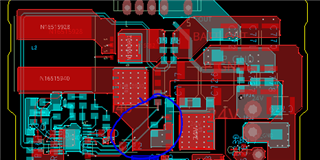
    I have one more Query need to Clarify from your side. This Query is regarding the PCB Layout. PCB is 6 Layer. Top Layer is for High current routing and bottom side layer used for LM5121 and associated circuit placement. Can I Route the High and Low side PWM Signal just under the switching Node through any of the Layer?

    Best Regards

    Saneesh

  • Hi Saneesh,

    This query does not relate to the device itself or the datasheet of the device, so I cannot suggest how to route your PWM signals, although I would suggest that the switching node is highly noisy with 400kHz as your switching frequency so I would suggest it to be not near the other critical components and have the ground close to this switching node. 

    BR,

    Haroon