This thread has been locked.

If you have a related question, please click the "Ask a related question" button in the top right corner. The newly created question will be automatically linked to this question.

LM2623: 5V to 12V design difficulties

Part Number: LM2623
Other Parts Discussed in Thread: LM2735

Hi TI

I am having trouble using the LM2623A to step up from 5V  (USB) to 12V with output current up to 500mA.

The issues I am having are:

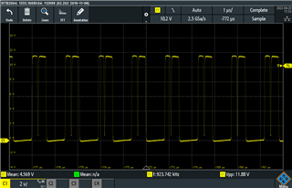
1) Large input current ripple causing big voltage ripple on the 5V input. The ripple is around 500mV pk-pk at 80-100kHz depending on the design/current load. 

I believe this is caused by the gated oscillator design. How can I minimise this ripple?

2) Double switching/pulsing at higher currents

No matter what values of R4 and C5 I choose, at higher currents I get double switching and sometimes triple switching where the fet turns on and off very fast. 

3) Current limiting early 

I believe related to 2). and varies according to R4 and C5

4) Trouble choosing the correct R4 and C5 values

If I lower C5, then I can't achieve the output current I need. If I raise it, then I get more double/triple switching. The same applies to R4. I have tried many many variations and 4.7pF and 180k seem to work best. 

5) Low efficiency

I am getting about 75-80% efficiency so the device and PCB is getting very hot. I believe this is related to the double switching at high currents. 

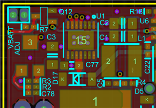
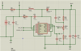
This is my schematic:

Thank you for any help you can give. 

Best regards

David

  • Hi David,

    Can you forward the PCB layout here for review? And can you take the waveforms of SW, Vbat, Vout, iL you described in 1)2)3)4). Thanks.

    Best Regards,

    Bryce

  • Hi Bryce, 

    Thanks for the reply. 

    There is a big 270uF low ESR cap on the bottom left which isn't on the schematic. I also appreciate that the position of the FB resistors isn't ideal. 

    I have set the output voltage (tested at low current) to 12.00V. So when I apply a 24ohm load it SHOULD allow me to output 500mA.

    This is my switching waveform when I apply a 24ohm load to VBATT. Here you can see the double switching. 

    In this condition:

    VBUS = 4.71V

    IBUS (current in) = 1.354A

    VBATT = 10.45V

    IBATT (current out) = 0.485 (435mA for the 24ohm resistor and 50mA for other circuits on the pcb)

    Eff % = 79.5%

    VBUS and VBATT are both stable in this condition so I haven't included the waveforms. 

    So what is going on here? Obviously current limiting of some sort I imagine. 

    -------------------------

    There is more to the story because this circuit forms part of a CC/CV battery charger so there is an external current limiting circuit. However, in the state above, this CC circuit was completely turned off. 

    I have 2k to need to get working. After this, I will give up with this IC and use LM2735 instead. I know where I am with a simple PWM controller...

    Thanks for your helps. 

    Best regards

    David

  • Hi David,

    Thanks for your detailed reply. As you mentioned, the layout of the FB resistor should be closed to FB pin.

    Followed are some of my advices you can try: 

    1. As the datasheet mentioned, incorrect C3 value may result in double pulsing which could lead to unstable output voltage. Unstable output voltage will also lead to unstable input voltage and furthermore affect the switching frequency. Current limit may also be triggered. Pls check the waveform of iL that peak current limit is not triggered.

    2. You can try to increase the R4 so the switching frequency can be smaller and thermal performance can be better.

    3. Try to remove C78 in case that it affects the loop stability.

    Best Regards,

    Bryce