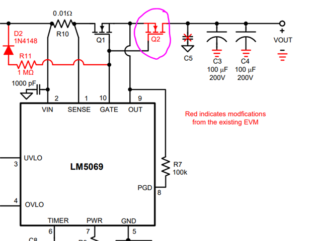
This thread has been locked.

If you have a related question, please click the "Ask a related question" button in the top right corner. The newly created question will be automatically linked to this question.

LM5069: Damaged LM5069 devices unable to control inrush

Part Number: LM5069

Hi,

I have a LM5069 design which is providing switching/protection of a nominally 48V output from a control card. In long-term running the design is fine but we've now had two device failures in power cycling testing with our load (after 300 cycles and 2000 cycles on different boards).

Once the device has failed an attempt at start-up (controlled by OVLO) results in a fault as the duration in FET power limit is exceeded. We originally suspected that the FET may have been overstressed but replaced the FET and still had the issue. We had to replace the LM5069 controller to correct it.

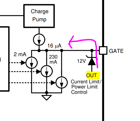
Investigation shows that the gate voltage driven by the "bad" controller during the power limited start-up phase is lower than on a "good" controller. As a result, the FET passes less current, doesn't manage to establish the output voltage in time and the controller goes into fault.

Please can you suggest potential causes of the damage to the controller that might yield such a symptom that we can investigate in the system?

Is there any other data that we can provide which would be useful in helping you to help us to identify the root cause of this failure, which we urgently need to resolve?

Many Thanks!

  • Hi Paul,

    Welcome to E2E

    Can you share the schematic and load details. When we do power cycling, the load capacitor gets discharged into the LM5069 and can stress the GATE section. Want to check whether that is the case here.

    Best regards,

    Rakesh

  • Hi Rakesh,

    Here's a link to the schematic, which I hope works for you (please let me know if not). 48V_IN is connected to a battery (could be 42-60V) and the switched output is +48V_BIAS which drives on-board and off board loads.

    Schematic Link

    I'm interested in your suggestion that the load capacitance could be discharged into the device. Our initial load for inrush and during a normal shutdown is as follows:

    - On-board PSUs with input capacitance 300uF

    - Remote motor driver (~5m cable length away) with input capacitance 1mF

    - 3x Fans whose inrush demand I'm not completely sure of.

    We're gathering more data from around the latest failed device which I should be able to provide soon.

    This is very urgent for us as it has high visibility so your urgent attention is appreciated.

    Paul.

  • Hi Paul,

    Thanks for the details. 

    From the failure description, it seems that there is leakage at the GATE node which can be due to partial failure of the pull-down sections or the ESD structure at the GATE. If we are controlling LM5069 using UVLO pin, then every time the Cout discharges through the GATE pull-down section which can stress the part. 

    Since the parts failed during power cycling test. Can you share the start-up, turn-off with UVLO=LOW waveforms to understand more. Please probe Vout, GATE and UVLO pin voltages.

    Best Regards,

    Rakesh

  • Hi Rakesh,

    We were beginning to think that this might be the issue, though it's hard to see how this wouldn't happen in almost any application. I guess that ours perhaps has more capacitance than most.

    See attached the traces requested:

     OneDrive_1_27-04-2022.zip

    - 02 - Startup showing UVLO rising, then GATE and VOUT (both measured with respect to GND)

    - 03 - Shutdown with the same signals. This shows that it takes around 2s for the load to be discharged on each power down.

    - 01 - Shows why the UVLO signal has a different voltage between the two traces above. It increases further in voltage once the second parallel opto-isolator which controls it is enabled.

    Paul.

  • Hi Paul,

    Thanks for the test results. It gives us clue now that why GATE is getting stressed during power cycling. If such frequent power cyclings are expected in actual use case, please use blocking FET in series as shown below.

    https://www.ti.com/lit/an/snva683/snva683.pdf 

    Best Regards,

    Rakesh

  • Hi Rakesh. Thanks for that. We're so advanced in our deployment of this solution that it's not possible to apply this retrospectively to our PCB design at this stage so we're looking at adding a series diode in the supply line to prevent the majority of the capacitance feeding back into the driver. 

    See the presentation here

    Diode comparison.pdf 

    We can use the diode to block 1mF of the 1.3mF capacitive load which will limit the duration that the LM5069 has to dissipate power through the GATE clamp.

    What do you believe would be an acceptable level of capacitance/energy dissipation in the device where we would not expect any damage to occur? There has to be some expectation of this happening as I don't think our use case is completely outside of what would be expected (though the capacitive load is high).

    I am running some representative fast cycling tests over the weekend on both the original and modified setups to see if we can stimulate/prevent failures. This should help to prove whether we have the right root cause or may need to look elsewhere.

  • Hi Paul,

    I will get back by early next week 

    Best regards 

    Rakesh

  • Hi Paul,

    Our design team still feels that it is too much stress for the internal pull-down to handle if power cycle happens frequently. The pull-down FETs are sized to handle 10's of mA current but for very short interval <50ms 

    I see less concern for input power recycling as Cout also discharge through the body diode of hot-swap to input side but in case of EN/UVLO cycling, the Cout will gets discharged only through internal pull-down of LM5069.

    Best regards 

    Rakesh

  • Hi Rakesh. Power cycling doesn't happen frequently in our application but we're trying to prove robustness over the lifecycle of the product where there could be thousands of UVLO power downs over many years.

    I've been power cycling 4 boards in the lab to try and recreate the failure and they have now completed 20,000 cycles of the UVLO input (14s ON, 7s OFF) without any parts failing!! This tells me that, whilst this may be applying stress to the part and may not advisable, this is clearly not the root cause of the functional failures we are seeing in our product where we've seen failures after 300 and 2000 cycles.

    We've done some more work to compare the operation of a part that has failed against a working part in the hope that you can help us to isolate what might have failed internally and therefore what event might have caused this damage. Please see the slides below

    Slides

    These show that the the failed part does not allow the FET to dissipate the power specified by the RLIMIT resistor until very late in the power-up cycle, compared to a working part which quickly reaches and maintains this level. We have validated the voltage across the RLIMIT resistor is the same and that the failed part seems to have a working current sense function (by checking current limit threshold once started) and a working VDS sense function (by checking when the PGD signal is asserted).

    We've also observed that the failed part is able to start into a load that it previously couldn't if we increase the RLIMIT value and that we can recreate a similar behaviour to the failed part on a working part if we reduce the RLIMIT value.

    Does that provide any clearer indications as to which part of the device might have failed/degraded and could you please suggest some possible causes so that we can investigate them?

    Thanks,

    Paul.

  • Hi Paul,

    Thanks for the update.

    The current limit is working fine in steady state and the power limit reference is also good. I am suspecting Vds function or the partial leakage at GATE node. 

    Can you confirm that the failed board was setting expected power limit (constant value like good unit) earlier just before you power cycling test ?

    Have you done A-B-A swap ?  Can you take out the units from the board and measure impedances at GATE and OUT pins for failed and good units to compare.

    One more test, I would like to perform is at different Vin levels (say 30V, 48V, 60V) on the failed unit to check whether power limit is still low.

    Best Regards,

    Rakesh

  • Hi Rakesh,

    I thought that the testing of the PGD output would also demonstrate that the VDS function sensing function is working properly. Do you think that is the case? I appreciate that increased GATE leakage does appear the most likely culprit but I'm interested in other options or things that might have caused that to be the case.

    I can't confirm that the power limit was fully correct on the units that failed before we started testing, as it's not something that we routinely test on all boards, but I have no reason to presume that it wasn't correct. 

    On the previous failed board we swapped the LM5069 and recovered correct behaviour (A-B test) but didn't then refit the failed part to check it was still dysfunctional (A-B-A). On the second failed board we have not yet changed the part. I'll build this A-B-A test and the measurement of the impedances of the GATE and OUT pins to GND whilst the part is off the board into the next steps of our test plan. I'll also ask for the tests to be performed at the high/low voltage thresholds as you suggest.

    As we've now done ~23,000 cycles on 4 boards with no failures I have been looking at other system-level events which might cause a situation which might affect the LM5069. I've captured what I found in the presentation below

    Slides

    Please review and see if there's anything of concern. Specifically on Slide 5, when we have a load on the battery (which is the input to the LM5069) the input voltage drops and so we get slightly negative Vds and negative currents flowing for a while whilst the LM5069 is enabled until the voltage recovers. This isn't an issue in the system and I don't believe it should be an issue for the controller but please confirm.

  • Hi Paul,

    PGD is a digital comparator output and cannot reflect if there is any issue in the power limit loop or power limit references

    I don't see any issue even in case of input voltage dips as long as it is higher than the UVLO threshold of LM5069.

    Regarding ~23,000 cycles on 4 boards evaluation, it is that done by reducing the Cout with a diode in the load path ?

    Best Regards,

    Rakesh

  • The input to the PGD comparator is the VDS sense output though I believe. So if we've seen the PGD output asserted at the right Vds threshold then wouldn't it suggest that sense is OK?

    The cycles have been done across 4 boards, 2 running in a configuration similar to our installation (all output capacitance connected) and 2 running with the diode isolating much of the output capacitance from being discharged through the LM5069.

    Paul.

  • Yes, VDS sense output seems to be OK as it is asserting at the right threshold

  • Hi Rakesh,

    OK - so we did the testing you requested. The results of which are captured in the presentation here

    Slides

    The summary is that the input voltage tests on the failed part show that higher input voltages fail to start even this low starting load because the device seems to be holding for Vds to reduce to ~40V before it ramps the power limit from ~35W it starts at to the target power limit of 120W. So when input voltage is >50V this takes too long and the fault timer (CTIMER=470nF=22ms) expires.

    The very interesting thing that we really cannot explain is that when we refitted the "failed" part back onto the same board (having tested a new part on it), it now works correctly! We have managed to apply high starting loads (both resistive and capacitive) and not seen the board fail to start again. I've now placed this board back onto our cycling rig to see if it will fail again after repeated starts.

    We removed the device from the board with a hot air device, soldered it with an iron to a test PCB for the resistance measurement, removed it from that PCB with hot air and soldered it back to the original board with an iron. We don't believe it could have been an issue with the actual solder joints when the device was originally fitted as the problem was very much degraded operation (as we've recorded here) rather than a digital fault as would be seen with a no connect.

    I've now also found the failed part from our first failed board so will be repeating some of these tests on that part today.

    Note that the part marking on both failed parts is "9902" and "SNAB"

    I'd appreciate any theories that would help to explain what we've observed so far ....

  • Hi Paul,

    Thanks for the further tests and A-B-A tests. It is making the case complicated as the failed unit started working when we soldered back. 

    Are all these units came with the same lot code ? These details are available on the packing cover

    Best Regards,

    Rakesh

  • The parts are all marked "9902" on the case as described above. Both failed devices have the same marking and are likely to be from the same batch as they were built at the same time. I don't have any of the packaging as these were built at our subcontractor many months ago. 

  • Hi Rakesh,

    We tested the board that failed previously and was fixed by changing the LM5069. We found the failed device and tested the board initially with the replacement part and having refitted the failed part and this one also was working correctly again once it was resoldered. Very strange!

    Here are the measurements taken including the traces we took of the board in its failed state back in December to show that it had the same behaviour.

    Slides

    Regards,

    Paul.

  • Hi Paul,

    Let me discuss with the design team and get back on what can be done

    Best regards 

    Rakesh

  • Hi Paul,

    All our devices goes out of production unit once it passed the automated test equipment (ATE). We are thinking whether the handling process during assembly onto your PCB or the soldering flow could have any impact. Can you look into those lines if we can any clue for the root-cause.

    Best regards 

    Rakesh

  • Hi Rakesh,

    I'm pretty sure that these boards only go through SMT reflow and that the profiles for that will be OK - though I'll check with the manufacturer.

    We're considering whether this could be caused by an environmental factor in operation either within the package or around the pins. The two boards that have failed boards have both been being operated outside in our test yard through operational cycling. The PCB is housed in an IP6-rated enclosure is not conformally coated and the temperature of the unit will have been varied from air temperature (say 0degC at times) to quite hot (say 60degC ambient) over the course of a few hours as the unit heats up and cools down. When in the system "OFF" state the unit is in the situation where LM5069 VIN is high and UVLO is held low so there remains a potential difference within/across the device.

    Are there any known/potential issues that could be caused by these conditions that would be fixed by remaking/cleaning the solder joints or by application of heat to the package during soldering?

    Thanks,

    Paul. 

  • Also note that the two devices that had failed and then started working again after refitting have completed over 6000 cycles of UVLO cycling starting into its normal capacitive load over the last couple of days in the lab. So whatever was causing it not to work before has certainly not returned with use.

  • Hi Rakesh,

    We have some more boards doing similar testing outside so we pulled those into the lab to run the same characterisation tests to see if they were degraded in any way.

    We found that one board which has been running constantly (i.e. LM5069 always enabled and at a relatively stable temperature) still operates normally. Another unit which has been doing power cycling (and therefore will have seen much greater thermal change) shows similar symptoms to the failed parts where the initial power limit is lower and then increases gradually. This board failed a higher start current test so it's likely it would continue to degrade until it fails. We plan to do some tests next week to see whether baking, cleaning or resoldering is the thing that causes this change in behaviour to reverse.

    Slides

  • Hi Rakesh,

    We've also done some testing with the board that we recently pulled off cycling which shows the same symptom of not applying the power limit correctly to start with but has not yet failed in the application.

    We wanted to check what operation would make the device improve this characteristic as the resoldering operation that fixed it before involved both temperature, cleaning and resoldering joints.

    We baked the board in an oven at 70degC for some time and took it out to recharacterise it at intervals and found that the longer the board was in the oven (and therefore the more moisture we removed) the initial power limit applied by the part increased each time. See the scope traces attached.

    Slides

    This would suggest that something (probably the LM5069 itself) is taking on moisture during operation and this is affecting the initial application of the power limit and that when the board is baked to remove this moisture it moves back to normal operation. Can you suggest any other possible explanations or discuss why this might be happening to these parts? We need to urgently understand the cause of these failures and how they can be resolved.

    Paul.

  • Hi Paul,

    Can we have a call to discuss more in detail. I will send you my contact details in private.

    Best regards 

    Rakesh