Other Parts Discussed in Thread: TINA-TI
Hi Sir,
my we learn from you,
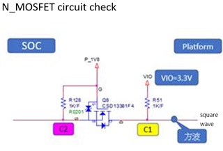
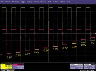
Refer to the following NMOS circuit diagram, input a square wave to the Drain terminal (point C1), and pull low from 3.3V==>0.1V, 3.3V==>0.2V, 3.3V==>0.3V, all the way to 3.3V==>1V
At the same time, looking at the change at the Source terminal (point C2), it can be seen from the figure that when the point C1 is 3.3V==>0.7V, there will be a relatively obvious offset voltage difference at point C2 (compared with the voltage at point C1)
What is this phenomenon? How to explain that there is an offset voltage difference, thank you for your help.