A related question is a question created from another question. When the related question is created, it will be automatically linked to the original question.
If you have a related question, please click the "Ask a related question" button in the top right corner. The newly created question will be automatically linked to this question.
Thanks for reaching out. Please kindly find my comments below:
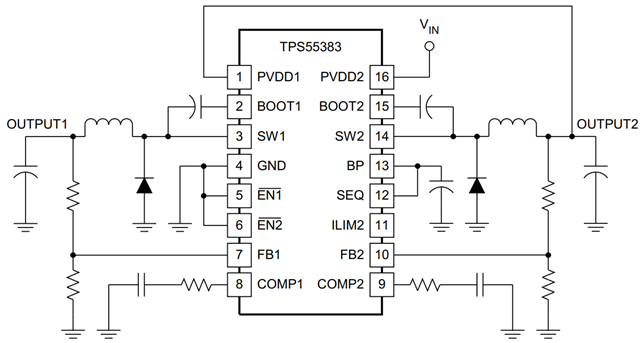
(1) Will PVDD1 and PVDD2 share the same input voltage? If I am understanding correct, input of Buck1 is from the output of Buck2?
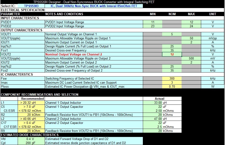
(2) I think the red mark is because of file setup error. I also tried in excel too and found that when VOUT2 is larger than 4.5V, this block will be marked as red. However, the output range of the converter is 0.8V to 90% of input voltage. You can ignore this red mark. TPS55383 can support Vin=24V and Vout=12V.
(3) In order to better verify this design, it is recommended to use TINA or Pspice simulation tool to verify the spec recommended by the excel tool and check the waveform.
Please kindly let us know if there is any more concern. Thanks!
1. My PVDD1 is like you said (it's come from VOUT2). I need to delay the Enable Pin of vout1?
2. Can I trust on simulation of TINA for the reliability my circuit?
3.In the simulation I have a problem when I keep the ILIM2 fly(The current limit is 3A in this situation) and RLoad require ~2A the output drop after 1ms.
I need to connect the ILIM2 to BP(The current limit is 4.5A in this situation) for solve the problem and I don't know why?
1. Do you use cascade supply shown below? If so, the following conditions need to be maintained:
(1) The voltage on output 2 is sufficient to support output1 before output1 is enabled. This requirement can be accomplished by a delay of the enable function or selecting sequential sequencing of output1 starting after output2 is in regulation. Which means that you need the delay enable pin of Vout1.
(2) The sum of the current drawn by Output 2 load plus the current into PVDD1 must be less than the overload protection current level of Output 2.
2. Yes, simulation results can be considered as reference and help you choose more suitable components. However, bench test is still needed to confirm it will work properly.
3. Which simulation tool do you use? Could you please send me your simulation file for me to better analyze this problem? What is your required output2 current limit?
4. Could I ask why do you choose this part? Is this a new design or do you choose it for some special features that you care about?
Thank you for the respond and I will answer about what you send me:
1.I connect the component as you described in your replay. So if I connect the SEQ pin to BP pin I don't need to put a delay in the EN pin?
2.can I do a test bench with TINA simulation ?
3.I use TINA simulation (my simulation is attached to my replay) my output current of Vout2 and Vout1 that require is 2A.but after what you said
in your replay I understood why the voltage drop when the over current was 3A.
Anyway if you could see my simulation and check if there are more mistakes I will very appreciate.
4.I choose this component for new design of power supply. If you have better component to offer me I will very appreciate. tps55383 - autosave 26-04-26 12_35.TSC
1. Yes, you can connect the SEQ pin to BP pin. In this condition, when output2 is enabled, output1 is allowed to start approximately 400us after output2 has reached regulation. That is, sequential startup where output1 is slave to output2. It will meet the cascade supply automatically. You do not need to add extra EN1 delay.
2. I think TINA can be used as a simulation tool. However, you still need to build evaluation board to verify your design from experiment view.
3. Nice to here that you solved your problem. I will also check your simulation and give you feedback soon.
Thanks! Feel free to let us know if there is any more concern.
I have reviewed your simulation file and I have some comments and suggestions shown below:
1. Do you have a requirement about board size? If yes, it is recommended to select 600k version which is TPS55386. You can also adjust design ripple current to decrease the value of the inductor.
2. An additional 0.1-uF capacitor from the Vin pin to GND is recommended to provide high frequency filtering.
3. For the output voltage resistor, we typically start with bottom resistor around 10k. Larger value resistor will be good to improve efficiency.
4. If you want to see the simulation results with output current, you can also add resistor load in the circuit. It is currently under no-load condition.
1. Switching frequency will have effect on the value of inductor, thus will affect the size of the inductor and the size of the board.
2. For example, if your load is 2A, output voltage is 5V, you can add a resistor between Vout and GND which is 2.5Ω. You can also add a current source which is 2A. It will also work.
No problem. Do you mean the tips to use this simulation tool? If yes, please kindly find the buttons shown below. If you want to add a resistor, you can directly drag it to your circuit. If you want other components apart from basic ones, you can click on Switches or Meters or sources and so on. You can find current source after you click on sources.
I'm sorry you got me wrong. I meant tips for edit the electrical circuit ,it's my first time with circuit editor and I don't know which details I need to pay attention