A related question is a question created from another question. When the related question is created, it will be automatically linked to the original question.
If you have a related question, please click the "Ask a related question" button in the top right corner. The newly created question will be automatically linked to this question.
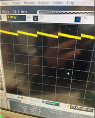
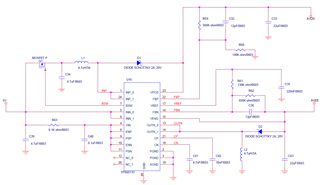
I reviewed the schematics and one change that I could suggest is to tie PSP/PSN (pin 9/11) to GND instead of Vin that it is currently tied to. When PSP is tied to Vin, boost can go into PFM mode during lighter load and can have a significant amount of ripple. For ripple sensitive applications, we recommend to tie PSP/PSN to GND so that the device stays in constant frequency PWM mode which has a lower and much stable ripple.
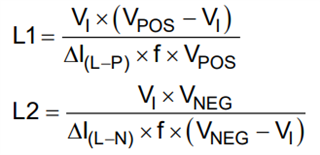
Increasing inductor value may help slightly but I would not recommend it as it may have some impact on loop stability and all validation on TI evm was also done with 4.7uH. I still suggest to tie PSP/PSN to GND to achieve lower ripple.