This thread has been locked.

If you have a related question, please click the "Ask a related question" button in the top right corner. The newly created question will be automatically linked to this question.

TPS54218: Differ the phase margin for Webench and datasheet equation

Guru 19575 points
Part Number: TPS54218

About TPS54218 setting compensation network based on datasheet equation (11)~(18), condition is below.

→Vin:5V, Vout:3.3V, Iout:1.3A, fsw:1.8MHz, L:2.2μH, Cout:22μF

 →R3 (Rcomp):10kΩ, C1 (Ccomp1):5.6nF, C2 (Ccomp2):2.2pF

When above value insert to Webench, but phase margin become low margin.

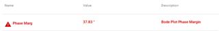
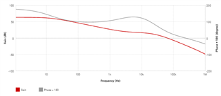
Webench report is shared below,

https://webench.ti.com/appinfo/webench/scripts/SDP.cgi?ID=424A3F69C1370892

Please let me know about the reason for gap by Webench and equation.

(Or, is these result Webench's bug?)

I thank that recommend to setting is based on equation (and actual measurement), is it correct? 

By the way, When TPS54218 board measured below condition, it was good transient response.

But Webench simulation was low phase margin. (Less than 40°)

R3 (Rcomp):15kΩ, C1 (Ccomp1):1nF, C2 (Ccomp2):Not mount

Best regards,

Satoshi

  • Hi Satoshi,

    I will look into this request and provide a feedback tomorrow.

    Regards,

    Febin

  • Hi Febin

    Thank you for reply,

    I looking forward your update tomorrow.

    Best regards,

    Satoshi

  • Hi Satoshi,

    I reviewed your design on Webench and made some modifications to the BOM and it works fine now. 

    https://webench.ti.com/appinfo/webench/scripts/SDP.cgi?ID=8AB2D9BC50067E12

    What I think is the actual problem is the choice of the passives. All the passive components should be properly chosen for the design to run correctly. Css, Cout, R_clk were modified according to the datasheet recommendations.

    Webench models are based on many approximations and estimations. Therefore; the actual measurement results will vary from the simulation results.

    My suggestion would be to perform Bode Plot measurements with the required BOM on the real PCB. If you get the required gain & phase margin, then you can proceed with the design (provided all the datasheet specifications are adhered to). Typically, if the phase margin is greater than 45 deg (preferable to include some buffer), then we can ensure that the device is stable.

    This device is pretty old and we recommend using one of our newer devices like TPS62851x or TPS62850x-Q1. The newer devices are easier to design, requires less no.of external components and are also better in performance.

    I hope this helps.

    Regards,

    Febin

  • Hi Febin

    Thank you for review and reply,

    I think that Webench and Datasheet equation have mismatch the calculation method of compensation network, is it correct? 

    Please let me know which consider mainly.

    Best regards,

    Satoshi

  • Hi Satoshi,

    It does not look like an equation mismatch but it is more like a modeling constraint. Please follow the datasheet.

    I suggest to perform Bode plot measurements on actual PCB for accurate results.

    This device is pretty old and we recommend using one of our newer devices like TPS62851x or TPS62850x-Q1.

    Regards,

    Febin

  • Hi Satoshi,

    Do you need further support on this issue? If not, I will go ahead and close this thread.

    Regards,

    Febin

  • Hi Febin,

    I apologize my reply delay.

    Thank you for support, I will close and resolve this thread soon.

    Best regards,  

    Satoshi