This thread has been locked.
If you have a related question, please click the "Ask a related question" button in the top right corner. The newly created question will be automatically linked to this question.
Hello,
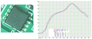
I have some questions about CSD25402Q3A.
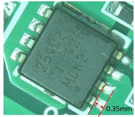
There is a problem that FET does not work properly due to poor soldering.
Here is the temperature profile that we used.
Do you think this temperature profile seem to be a problem?
The lead on the drain side doesn't seem to melt well.
I looked at the temperature profile in the data sheet, and there doesn't seem to be any problem in our temperature profile.
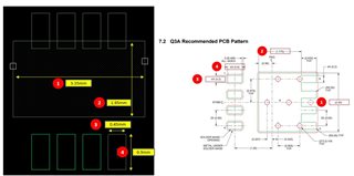
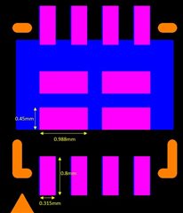
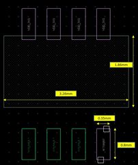
Can a metal mask or library cause this problem?
Thanks a lot.
Hi Rona Lee,
Thanks for the inquiry. Have you followed TI's recommended PCB and stencil patterns in the datasheet? Are you using SMD or NSMD pads? What is the solder paste used for assembly? Please refer to the app note in the link below for more details on attachment of these devices. I will ask our SMT expert to review this as well.
https://www.ti.com/lit/an/slua271b/slua271b.pdf
Best Regards,
John
Hi Rona Lee,
I followed up with our SMT expert and his feedback is given below. Can you share more details of the PCB footprint used?
From TI SMT expert:
I don’t see any major issue from the reflow profile. The length of the PCB pads seems to be quite long. Our recommendation is 0.2mm longer than the component lead. It seems the PCB pads extend more than 0.2mm from the end of the leads. The longer PCB pad means providing more space for the solder to flow. If the component placement push the package too close to the PCB surface, then solder paste got push outward and end up insufficient solder under the leads.
On top of the question you asked about the PCB details, please ask the customer about the component placement detail. Like how much force was used or what is the release condition if the placement used package thickness.
Best Regards,
John
Hi John Wallace,
Thanks for your assistance.
I used NSMD pads.
TI recommendation is 0.2mm longer than the component lead.
It means that the length between edge of pin and pad ? The length is approximately 0.35mm.
Should the solder mask be modified to reduce solder mask opening size ?
I didn't follow stencil patterns in the datasheet.
Here is solder mask.
I don't know exactly, but manufacturer told me that the component had very little force to push the PCB out.
Are there any other recommended force values?
I don't fully understand TI's answer as my native language is not English.
Please understand me if I ask same questions for understanding.
Thank you,
Rona
Hi Rona Lee,
Thanks for providing additional information. We have reviewed and feedback is given below.
Rona only told us they used NSMD and provide the solder mask opening. That didn’t shown much on the PCB pad size. Can you ask them for the gerber file if available. Or at least provide the PCB soldering pad dimension.
For component placement, there are two ways they can release the package. One is by force, we recommended to use around 3N. Another way is to use package thickness, we recommended to use actual thickness + 0.05mm. That will put the package into the middle of the solder paste.
Best Regards,
John
One more request: we also need the stencil (gerber) file or at least the stencil aperture (opening size).
Hi John Wallace,
Thanks for the further checking.
Here is stencil aperture.
Here is PCB pad size.
Is this what you want ?
Hi Rona Lee,
I have shared this information with our SMT expert. I am still waiting for his response. I will update you when I have more information.
Best Regards,
John
Hi Rona Lee,
Below is the feedback from our SMT expert. Please let me know if you have any additional questions.
I compare the PCB and stencil information from GGI
to TI recommendation (see below table).
The I/O solder coverage was fine but the thermal pad
area was extremely low. During reflow, the package would
be pulled towards the PCB surface pressing the solder
at the I/O pins. Since the PCB pad for the I/O pins
are quite long and have extra space outside of the
package footprint, part of the solder will flow
out of the package footprint. As a result, the
package could be tilted or have less solder underneath
the package.
Recommendation is to increase the solder coverage
at the thermal pad area to maintain a balance.
TI PCB Pad |
TI Stencil |
TI PCT Coverage |
GGI PCB Pad |
GGI Stencil |
GGI PCT Coverage |
|
Pin 1-4 |
0.3 X 0.6 |
0.3 X 0.6 |
100% |
0.35 X 0.8 |
0.315 X 0.8 |
90% |
Pin 5-8 |
0.3 X 0.635 |
0.3 X 0.6 |
94% |
0.35 X 0.8 |
0.315 X 0.8 |
90% |
Thermal Pad |
2.45 X 1.775 |
1.125X0.705X4 |
73% |
3.26 X 1.86 |
0.988 X 0.45 X 4 |
29% |
Best Regards,
John