This thread has been locked.

If you have a related question, please click the "Ask a related question" button in the top right corner. The newly created question will be automatically linked to this question.

UCC2803: Design help with UCC2803 controller IC

Part Number: UCC2803
Other Parts Discussed in Thread: , LM431, UCC2813-0, UCC2800

Hi Team,

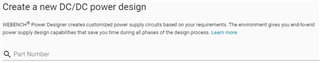
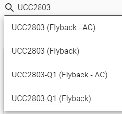
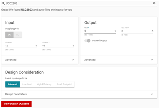
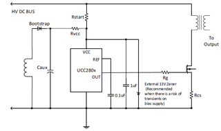
Could you help our customer and clarify the usage of UCC2803 controller IC.

Here is their concern:

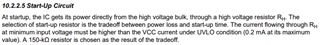
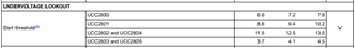
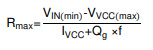
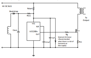
"There is an input resistance mentioned as RH which is connected between input voltage and VCC pin Besides, there is a formula on how to calculate the maximum R for the minimum input voltage in the datsheet However, I have one doubt regarding the working of IC. Will this controller IC UCC2803 will successfully work for Input DC voltage varying from 12 V to 80 V. Because there is i think minimum input DC voltage requirement for IC to work And if I use 12 V as minimum voltage then according to the formula of Rh the resistance value is in negative Is it possible to know how to exactly regulate this controller IC. I am using this IC to produce dual secondary voltage. But, how exactly regulation works and how can I set it is still not found yet. It will be helpful if I can get to know how exactly to regulate the flyback controller"

Looking forward to your response. Thank you in advance. 

Best regards,

Jonathan

  • Hello Jonathan,

    The 13.5V zener diode will normally be off.  I responded to the customer about this in another E2E thread:  here.

    If your want a little more details on how to calculate RH we have to understand this section of the datasheet.

    At the minimum input voltage, the RH resistor must allow at least 0.2mA to the UCC2803 without causing the VCC pin to drop below UV_start.  So the formula would be RH = (Vin_min - UV_Start_max) / 0.2mA = (12V - 4.5V) / 0.2mA_max = 37.5kohms.

    I will edit the customer's post with this additional detail.

    Regards,

    Eric

  • Hi Eric, 

    The formula which you have used to calculate RH doesn't resemble with the one shown in datasheet. However, I will go with the one which you have shown. And can I use the same formula with varying input (minimum) voltage to design the resistance value?

    Besides, I want to know can I use this controller in form of primary sided regulator (PSR based flyback) application? and if than how because the refernce is not provided in any application note. 

  • Hi Ravi,

    Are you referring to equation 7?  This formula assumes the most basic use of the regulator from a single supply where the 13.5V zener would be always active, like the boost topology shown on page 1 of the datasheet.

    For a flyback topology there is usually an AUX winding to supply VCC after startup.  Before startup, there needs to be a way so supply VCC from VIN because AUX will be 0V.  So you need 2 resistors, as shown in figure 11-1 from the datasheet, and copied below.  The formula I provided yesterday is for Rstart1.  Rvcc value must satisfy Rmax equation with VINmin being your minimum AUX voltage.

    As for how to use it in a PSR based flyback that's addressed several ways.

    First, and easiest method, is to use Webench tool on TI's web site.  Start to type UCC2803 in the "Part Number".

    Select UCC2803 (Flyback) or UCC2803-Q1 (Flyback) from the Part Number pull-down menu.

    Enter your Input voltage range, Output voltage, and Output current.  You cannot turn off "Isolated Output".

    This will show you an isolated design with Secondary Side Regulation (SSR), but it's a starting point.  Note that your can use Export to save or print a detailed report on the design.

    The challenges would be to add a sense winding (or use the AUX winding), and remove the output opto-couppler and LM431, add an output voltage divider, and move the compensation to the FB/COMP pins of the error amplifier.

    Attached is a PDF of a HV flyback EVM I am working on that is about to release.  It is a PSR flyback, so you can at least see the basic circuit structure.  This circuit uses the predecessor to the UCC2803, so it does not have built in soft start or leading edge blanking.

    HVP066E1(Default)_Sch.PDF

    You can also search TI's extensive list of reference designs to see if any are close to your specifications,

    https://www.ti.com/reference-designs/index.html

    Lastly, there are many resources on the internet if you Google something like "PSR flyback design".

    Regards,

    Eric

  • Hi Eric,

    Thanks for detailed explanation. However, When I use the calculated value for Rstart (37.5 kohm) in my simulation, the simulation runs or completes without producing any results. And when I omit that particular resistor or place a small value resistor, it runs perfectly. As of now below is my working conditions:

    Vaux = 18V fixed

    Vinput = 18V to 80V (initially 12 V was considered as min input)

    Two secondaries are acting as a load.

    Kindly provide some insight on this condition.

    Thanks

  • The below mentioned errors are showing up while simulating in SIMetrix with model UCC2813-0 in which I am using the resistor value which you have shown in calculation. And other models are not available and the one which are available show the error of encryption.

    Device UCC2813-0 found in C:\Users\E0687541\Downloads\slum512\UCCx800_UCCx813-0_PSPICE_TRANS_UNENCR_18FEB2016\uccx813-0.lib

    Device UVLOX2 found in C:\Users\E0687541\Downloads\slum512\UCCx800_UCCx813-0_PSPICE_TRANS_UNENCR_18FEB2016\uccx813-0.lib

    Device FETOUTC4X found in C:\Users\E0687541\Downloads\slum512\UCCx800_UCCx813-0_PSPICE_TRANS_UNENCR_18FEB2016\uccx813-0.lib

    Device ZEN13p5 found in C:\Users\E0687541\Downloads\slum512\UCCx800_UCCx813-0_PSPICE_TRANS_UNENCR_18FEB2016\uccx813-0.lib

    Device OR2380x found in C:\Users\E0687541\Downloads\slum512\UCCx800_UCCx813-0_PSPICE_TRANS_UNENCR_18FEB2016\uccx813-0.lib

    Device COMPAR380x found in C:\Users\E0687541\Downloads\slum512\UCCx800_UCCx813-0_PSPICE_TRANS_UNENCR_18FEB2016\uccx813-0.lib

    Device INV380x found in C:\Users\E0687541\Downloads\slum512\UCCx800_UCCx813-0_PSPICE_TRANS_UNENCR_18FEB2016\uccx813-0.lib

    Device AND2380x found in C:\Users\E0687541\Downloads\slum512\UCCx800_UCCx813-0_PSPICE_TRANS_UNENCR_18FEB2016\uccx813-0.lib

    Device UTD380x found in C:\Users\E0687541\Downloads\slum512\UCCx800_UCCx813-0_PSPICE_TRANS_UNENCR_18FEB2016\uccx813-0.lib

    Device LATCH380x found in C:\Users\E0687541\Downloads\slum512\UCCx800_UCCx813-0_PSPICE_TRANS_UNENCR_18FEB2016\uccx813-0.lib

    Device COMPARHYS found in C:\Users\E0687541\Downloads\slum512\UCCx800_UCCx813-0_PSPICE_TRANS_UNENCR_18FEB2016\uccx813-0.lib

    Device NAND2380x found in C:\Users\E0687541\Downloads\slum512\UCCx800_UCCx813-0_PSPICE_TRANS_UNENCR_18FEB2016\uccx813-0.lib

    Device LATCH_HD found in C:\Users\E0687541\Downloads\slum512\UCCx800_UCCx813-0_PSPICE_TRANS_UNENCR_18FEB2016\uccx813-0.lib

    Device COMPARCS found in C:\Users\E0687541\Downloads\slum512\UCCx800_UCCx813-0_PSPICE_TRANS_UNENCR_18FEB2016\uccx813-0.lib

    Device AMP3802 found in C:\Users\E0687541\Downloads\slum512\UCCx800_UCCx813-0_PSPICE_TRANS_UNENCR_18FEB2016\uccx813-0.lib

    Device OR3 found in C:\Users\E0687541\Downloads\slum512\UCCx800_UCCx813-0_PSPICE_TRANS_UNENCR_18FEB2016\uccx813-0.lib

    Device COMPARX1 found in C:\Users\E0687541\Downloads\slum512\UCCx800_UCCx813-0_PSPICE_TRANS_UNENCR_18FEB2016\uccx813-0.lib

    Device FFLOP380x found in C:\Users\E0687541\Downloads\slum512\UCCx800_UCCx813-0_PSPICE_TRANS_UNENCR_18FEB2016\uccx813-0.lib

    Device NAND380x0 found in C:\Users\E0687541\Downloads\slum512\UCCx800_UCCx813-0_PSPICE_TRANS_UNENCR_18FEB2016\uccx813-0.lib

    Device NAND380x1 found in C:\Users\E0687541\Downloads\slum512\UCCx800_UCCx813-0_PSPICE_TRANS_UNENCR_18FEB2016\uccx813-0.lib

    Device INV380x1 found in C:\Users\E0687541\Downloads\slum512\UCCx800_UCCx813-0_PSPICE_TRANS_UNENCR_18FEB2016\uccx813-0.lib

    Device LMlatch380x found in C:\Users\E0687541\Downloads\slum512\UCCx800_UCCx813-0_PSPICE_TRANS_UNENCR_18FEB2016\uccx813-0.lib

    Device AND2BLM found in C:\Users\E0687541\Downloads\slum512\UCCx800_UCCx813-0_PSPICE_TRANS_UNENCR_18FEB2016\uccx813-0.lib

    Device INVBLM found in C:\Users\E0687541\Downloads\slum512\UCCx800_UCCx813-0_PSPICE_TRANS_UNENCR_18FEB2016\uccx813-0.lib

  • Hi Ravi,

    What is the end time of the simulation?  When you use 37.5 kohms there will be a long time constant formed by this resistor and the capacitor on VCC pin.  For example, 37.5 kohms and 1 uF create a 37.5 ms time constant.  So you have to simulate to 4x or 5x time constants.  Or, speed things up by using a smaller Rstart, but keep in mind this resistor is lower value.

    Eric

  • Those errors don't tell us much.  Is there more information before or after the list is produced that would provide more insight?

    Did you import the model into Simetrix somehow before using it?

    Eric

  • the simulation is running for 20ms. However, after trying with certain variations, same error appears in the Simetrix simulation. Besides, Pspice also shows a similar type of error. In Pspice, the output voltage at the secondary sides results in 0V even when the simulation time is 100ms and RH=54k and aux resistor Rvcc=177.

    Also, is there any reference for DCM mode with this IC's to verify, because that kind of data relative to this group of IC can help.

  • Hi Ravi,

    I'm a bit confused now:  Pspice errors, Simetrix errors, when do these error occur, etc.

    Here is what I would do in Pspice (based on my Pspice experience):

    1. See if there is an option to Skip DC Operating Point, only run transient simulation
    2. Set initial conditions of 0V on critical capacitors (SS, output, input), and 0A in inductors
    3. Use a transient step function for VIN supply, not a DC input
    4. Set maximum time step to 10ns, 50ns, 100ns, etc. (Pspice tries to have huge timestep and misses switching events)

    I don't understand your question about reference for DCM mode.  There are hundreds of good discussions on the internet about DCM Flyback design:

    https://www.ti.com.cn/cn/lit/an/snva761a/snva761a.pdf?ts=1651687023617&ref_url=https%253A%252F%252Fwww.google.com%252F

    https://www.powerelectronicsnews.com/design-features-of-a-dcm-flyback-converter/

    https://www.researchgate.net/publication/336033820_Design_of_a_22_W_07_A_Current_Controlled_DC-DC_Flyback_Converter_Operating_in_DCM_Mode

    Eric

  • Hi Eric,

    All of your responses were highly useful. Considering all the available data, I have verified my simulation in Pspice. I just want to confirm few things from you.

    1. In my current requirement input voltage variation is from 18 to 40 V and the auxiliary voltage rating is 18V. From these two voltages, I have finalized the resistance values of both the resistors. One is Rvcc and other is Rstart as mentioned in below diagram.

    For Rvcc as per my understanding and a reference document available on TI website it is calculated as below:

    Rvcc = (Vmin-Vcc)/(max operating supply current + supply current required for external mosfet)

             = (18-12)/(1mA + 4mA)    (here as per the reference document, 12 V is taken)

    Rvcc = 4.29 kohm

    Link for the reference document: https://www.ti.com/lit/an/slua081/slua081.pdf ts=1651946940629&ref_url=https%253A%252F%252Fwww.ti.com%252Fproduct%252FUCC2800

    In case of Rstart, we have to consider the UVLO of the controller IC. In my case UCC2800 is having 7.2 V start UVLO and in this case on startup current should be considered i.e., 0.2mA as per datasheet.

    Rstart = (Vmin-UVLO)/0.2mA = (18-7.2)/0.2mA = 54kohm

    Question: Are the above value considered for calculation of resistance such as 12 V (Vcc) in Rvcc and UVLO in Rstart are viable or not?

    2. Now as per the provided example, the location of Cvcc2 that holds initial voltage and its value finalization is still unknown. Can you please show some insight on its location (i.e., before or after  Rvcc) and its value. As the location of Caux in upper image and Cvcc2 contradicts. Kindly show some insights on that too.

    3. I also want to know what is there any current consumption in FB pin from auxiliary winding?

    Kindly provide me your suggestions on above calculations as per my requirement. 

    After placing all the components as per the above mentioned calculations, below are the results. The flyback is configured as PSR flyback.

    4. The w/f shown below is with Rvcc = 4.3k, Rstart = 54k and Cvcc2 = 5u. As it can be seen startup delay is much more (250ms) and the IC stops working after few ms.

    5. The below w/f shows Vcc voltage with Rvcc = 500ohm, Rstart = 54k and Cvcc2 = 5u. Here the controller IC works perfectly after start up delay. But the current from resistor Rvcc is very high having peak of 50mA, which is not ideal as per the datsaheet.

    Considering all the above mentioned results, what should be the considerations for finalizing values of these components considering practical implementation.

  • Hi Ravi,

    1)  The formula for Rvcc is "maximum" value if the IC is operating of a DC input as shown in Figure 1.

    In fact, the VCC pin can support up to 30mA.  So if you want a minimum value (Rvcc_min) use 20-25mA in the formula for Rvcc.

    With the exception for Rvcc_min, the formulas for Rvcc and Rstart look OK to me.

    2) The VCC pin in the picture you provided has 2 capacitors, Cvcc1 and Cvcc2.  Both capacitors must be connected directly to the VCC pin.  Cvcc1 is a 1uF ceramic capacitor that must be placed near the VCC pin to remove high frequency noise.  Cvcc2 is a 120uF hold-up capacitor that can be placed "near" the regulator.  Cvcc2 charges up and must prevent the VCC pin from dropping below the Stop threshold until the AUX can rise high enough to take over.

    3) Size Cvcc2 to provide the ICs current for the soft start time.  Think I = C dV/dt and solve for C.  Where "I" is the input currents (1mA+4mA, or more), C is Cvcc2, dV is the minimum Start to Stop threshold (4.1V - 3.6V, allow some margin, maybe 50%), and dt is the soft start time for AUX to rise above the Stop threshold.

    The FB pin does not consume much current, much less than 1uA per the datasheet.

    4) This simulation stops working because the VCC hold-up capacitor is only 5uF.  The VCC pin voltage is dropping below the Stop threshold.  You must increase the VCC capacitance(s).

    5) VCC pin can take more current provided the 13.5V zener at the VCC pin is off (i.e. VCC < 12V).  Note that some of the Rvcc current is charging the capacitor at the VCC pin, so all current is not going into the regulator.  I think the Rvcc peak current would be reduced if VCC capacitance(s) were increased.

    Eric

  • Hi

    This is regarding the controller IC UCC2800 on which the discussion was going on. I have a doubt regarding the noise on the input pin of VCC. Below is an image of the noise at the VCC pin. As you can see noise (spikes) at every 100 kHz is observed. Besides, the flyback is working in DCM at 100 kHz switching frequency. And the avg value of the input current at VCC pin is less (13.5 mA), but spikes of upto 200 mA are observed. What can be the potential source of this spikes and how can I mitigate it?

  • I thought you were using the UCC2803.  Now you ask about the UCC2800.

    In any case, it's difficult to diagnose without a detailed schematic.  The most likely cause of the spikes is gate drive current to the MOSFET.  Are you using a gate drive resistor between the OUT pin and the gate of the MOSFET?

    This is a simulation.  You should be able to place probes throughout the circuit to pinpoint where this current is going.

    Eric

  • When it comes to functionality both UCC2803 and UCC2800 works the same way, few differences are there such as 100 % duty cycle and UVLO. So, it doesn't make difference.

    I have used Rg to drive the mosfet. There is no other point where this noise is prevailing.