This thread has been locked.

If you have a related question, please click the "Ask a related question" button in the top right corner. The newly created question will be automatically linked to this question.

UCC27516: High-side configuration

Part Number: UCC27516
Other Parts Discussed in Thread: UCC27614, UCC27322

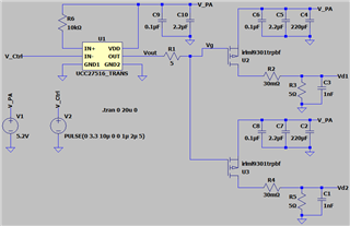
I need a gate driver for a front end power amp switching application - A Power MOSFET switches the drain bias of a PA on and off with a p-channel MOSFET configured as a high-side switch. I was considering using the UCC27516/7 but the application descriptions only mention low-side use. As far as I can tell, there doesn't seem to be a reason why this couldn't work for a high-side P-Channel MOSFET. In fact, Spice simulations seem to show that it works when I set the device up in an inverting mode.

Am I missing something? Will the UCC27516/7 performance be undesirable in some way?

  • Hi Ryan,

    Thank you for reaching out on E2E!

    You can indeed use a low side driver as a high side switch! A link to to an FAQ regarding using it as a high side switch can be found here: https://e2e.ti.com/support/power-management-group/power-management/f/power-management-forum/1082920/faq-ucc27624-can-i-use-a-low-side-driver-as-a-high-side-driver?tisearch=e2e-sitesearch&keymatch=driving%25252525252520a%25252525252520pmos%25252525252520with%25252525252520low%25252525252520side#

    However, there are some consideration to take into account when using a PMOS switch. During a UVLO event, the output of the driver is held low which will leave the PMOS on causing the switch to burn up. It is not advisable to use a PMOS switch in this case.

    Can you provide me with a schematic of your design? This way I can take a look and give you some recommendations to optimize switching on the high side.   

    Thank you,

    Kevin

  • Hi Kevin,

    Thanks for the reply. That's a helpful link as well. 

    Your point regarding UVLO is fair, I hadn't been giving that as much though but I think it may be ok in this application. To be clear, this isn't for a regulator design. We have a PMOS being used to quickly shut a front-end amplifier on and off.

    Here's a snapshot of the Spice model. Please excuse my use of LTSpice, haha. Nothing against TINA or TI PSpice (I use them as well), I just happened to have LTSpice already setup for these designs.

  • Hi Ryan,

    Thank you for getting back to me!

    No worries on using LTSpice I have used it plenty before!

    I will get you a response to this tomorrow.

    Thank you,

    Kevin

  • Hi Ryan,

    Thank you for your patience!

    There are a couple of suggestions that I have regarding the current design.

    Firstly, I would highly advise that you move away from PMOS FETs and switch them to NMOS FETs. Almost all modern day gate drivers have UVLO protection, which will cause the issue mentioned above with the PMOS always being on during an UVLO event.

    Switching to an NMOS FET, you must move your dissipation resistors R5 and R3 above your switch. If you keep a large resistance below the NMOS switch, a voltage drop could occur which will lower the gate to source voltage(Vgs). Imagine we have a FET with a turn on voltage of 10V. If you apply 10V to turn on your FET, and there is a 5V drop across that resistor, your Vgs will be 5V which could not be enough to fully turn on the FET.

    When paralleling two switches, you should implement a gate resistor for each of your FETs. Giving each MOSFET its own gate resistor rather than one gate resistor for all of the paralleled MOSEFTs, minimizes the ability for the individual MOSFETs from coupling noise onto each other’s gates.

    Below is an example using UCC27614 with two paralleled MOSFETs.

    Based on the other thread, UCC27614 will be your best option in terms of drive strength since you are going to be paralleling these two NMOS FETs which double your gate drive load capacitance. For the moment you can use UCC27322 SPICE model as a simulation tool. Just be aware that UCC27322 can sink and source 9A/9A and UCC27614 can sink and source 10A/10A.

    If you have any further questions or would like more explanation on this, please let me know. I would be happy to help you look more into this or any other TI low side/GaN gate drivers!

    Thank you,

    Kevin

  • Hi Kevin,

    Thanks for the suggestions. We're definitely look closer at the UVLO conditions. That said, I think that higher level system controls/monitoring should prevent burnout of the MOSFET. Additionally, at this time changing to a PMOS would require further redesign not scoped for the current effort. 

    I will follow your suggestion of simulating with the UCC27322 model.

    Thanks!

  • Hi Ryan,

    Gotcha! Thank you for the update. If you need anything else please let me know!

    Thank you,

    Kevin