Other Parts Discussed in Thread: UCC28780

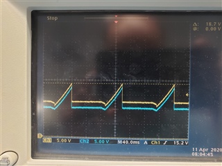
Above screenshot is the startup test waveform on Q2' Source and Gate in UCC28780EVM-02 . The ramp-up time is around 50ms.
We prototyped the circuit with Q2 replaced by BSP135 and the same capacitance 40uF on VDD. The new circuit uses extra 2.5mA from VDD for other circuits. We found the time on ramp-up waveform is increased to 4.5 seconds. In Fig. 16 of datasheet SLUSD12A, the statement is described below
RDDS is set at 12 kΩ when VVDD is below 1 V to limit the maximum fault current under VDD pin short events. RDDS is reduced to 1 kΩ when VVDD rises above 1 V to allow VVDD to charge faster. The maximum charge current (ISWS) is affected by RDDS, the external series resistance (RSWS) from SWS pin to QS, and the threshold voltage of QS (VTH(Qs)).
Question: The 4.5-second ramp-up time is due to damaged RDDS remaining at 12 kΩ even VDD is above 1V ? Or due to QS (VTH(Qs)) is reduced under higher initial charge current of Isws which is limited by the equation of VTH(Qs)/(RDDS+RSWS)?

