

Hi team,
My customer confirmed the internal structure by X-ray.
Then, the solder inside seems to flow and stick.
Is this a problem as an internal structure?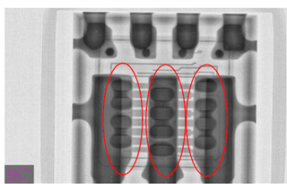
Sincerely.
Kengo.

-
Ask a related question
What is a related question?A related question is a question created from another question. When the related question is created, it will be automatically linked to the original question.
