This thread has been locked.

If you have a related question, please click the "Ask a related question" button in the top right corner. The newly created question will be automatically linked to this question.

LM25117: VCC pin spike problem consultation

Part Number: LM25117


Dear experts,

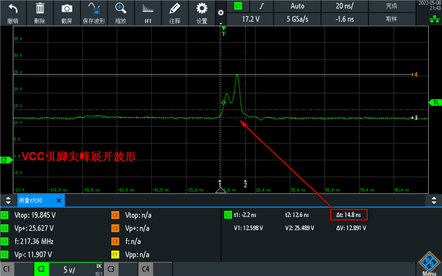
When using LM25117PMHE/NOPB, It is found that the VCC pin of the power chip has a spike that is frequently consistently with the driving frequency of the MOSFet  (≈221kHz). The value of spike is about 25V. And the duration is about 12ns. The peak appears at the same time when the upper tube is turned on. The waveform and circuit are shown in the attachment;

Since the diode D47 is connected in series between the VCC pin and the capacitor, it cannot be removed, and it cannot be replaced with a 0Ω resistor due to the special package. Based on the current circuit, is there any suitable BOM rectification measures to adjust the peak? Or does the spike have any effect on the application and life of the chip, thank you!

  • Ch1 is VCC pin waveforms.CH3 is upper switch VGS waveform.

  • Hello Zoe

    I think you have to double check if any noise coupling when you measure the VCC pin voltage, or if any ground bouncing. 

    Because the Abs Max of the VCC pin is only 15V, the VCC regulator would be damaged if the ~26V spike is real. 

    Please use only one probe and measure between the VCC capacitors. 

    - Eric Lee 

  • Thanks for the input based on E2E. I have forward your suggestion and now I have feedback from customer side. They re-test the VCC by using differential probe and the spike is still here. You mentioned our Vcc regulator cannot withstand 26V if the spike real exist.

    Zoom in the timeline, the duration of the spike is only around 17ns in the full load @4.1A output.

    When @light load, Vcc pin waveform shows 280ns duration on the spike.


    So Inovance conclude :From the waveforms measured above, it is found that the spike width is larger and the amplitude is smaller at light-load; the spike width is narrowed and the amplitude is increased at full load. But both  the frequency is consistent with Vgs. But the peak appears when the upper tube is closed at light-load stage, which is not the same when the spike occurs when the upper tube is turned on at full load; as shown in the following figure(Ch1 is VCC pin, ch2 is SW,ch3 is upper switch VGS)

    They conduct another experiment to replace Schottky to a Fast recovery diode at D1. The spike also appears at upper switch turn on period.  


    Support need:

    • They wonder if the real existing 26V within 17ns~280ns could damage our device?
    • Since one way of eliminating this spike is to put a capacitor between VCC and GND. Their current schematic has a diode between GND and VCC, and of which diode’s package is special and cannot be replaced by a 0ohm resistor.
    • Do we have any suggestions on eliminating this spike? If not, would this be a risk for system reliability of existing this kind of spike?


  • Hello Zoe

    Yes, the VCC pin can be damaged by the 26V spike if it is real. But, I think your customer didn't measure the voltage between the VCC pin and the AGND pin. 

    If possible, please move C82 or C84 very close to the IC and measure the voltage between the VCC pin and the AGND pin again. 

    - Eric Lee

  • Hello
    I am closing this thread since I have not heard from you for sometime.
    If you are still trying to resolve the issue, please feel free to open a new thread or reopen this thread. Thanks
    - Eric Lee (Applications Engineering)

  • Eric, 

    In the datasheet ,the minimum SW to AGND is -3V. 

    But in customer testing waveform we can find out the negative voltage on the SW pin goer larger when the load getting heavier. See below waveform.

    The time to exceed the -3V specification was found to be 9.4ns as shown in the following waveforms. And the measured minimum value is -4.2V.

    Should the overshoot of this SW pin be strictly controlled within -3V and cannot be exceeded? Or is there a time requirement for the specification of the SW pin? If the specification exceeding -3V, is it acceptable as long as it meets the requirements within a certain period of time? If so, can you provide the relevant time for reference; is there any reliability or application risk, thank you!

  • Hello Zoe 

    I cannot guarantee anything outside of datasheet limits. You can make the negative spike smaller by making the switching loop smaller. Please  place a input ceramic capacitor close  to your MOSFETs and current sense resistor.  

    - Eric Lee