This thread has been locked.

If you have a related question, please click the "Ask a related question" button in the top right corner. The newly created question will be automatically linked to this question.

UCC28019: PFC Circuit PFC Circuit Unidentified Error

Part Number: UCC28019
Other Parts Discussed in Thread: TIDA-010080, TPS5431

Design Parameters

Parameter

Min

Nom

Max

Vin

90 V

230 V

265 V

Fline

47 Hz

50Hz

63 Hz

Vout


390 V


Iout


1,795 A


Pout


700 W


Vcin_ripple_factor


0,07


Li_in_ripple_factor


0,4


Over Voltage Protection


410 V


Undervoltage Protection


370 V


PF


0,99


Holdup time


20 ms


Fsw


65 kHz


Efficiency


0,92


Chip

UCC28019

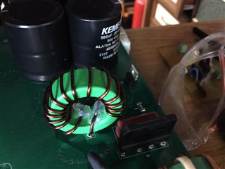
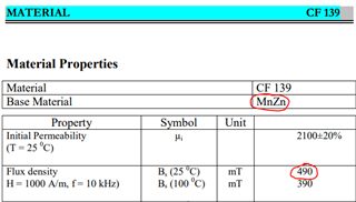
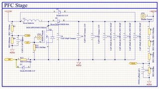
By using the above target parameters, the boost converter topology and the boost pfc circuit were designed. The "sluc069e" calculator was used in the system design. In the system, a 0.6 mH coil with my own winding is used against the minimum boost coil value of 0.311 mH in the calculator (The image of the coil is attached). The EMI filter structure suggested in the UCC28019 datasheet is used at the system entrance. Images are as follows.

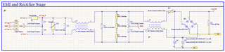
The system mentioned above will then feed the LLC Half bridge topology. The whole system is on the same printed circuit board. However, only the PFC circuit will be assembled and the PFC and EMI circuit will be tested and the next stage will be passed.

While testing the EMI and PFC structure, which is the first part of the system, the following situations were realized respectively. No load is connected to the system during testing:

In the first part of the system, the power supply stage given below is fed from the network. A voltage of 14.6 V DC was observed at the output. UCC28019, which is a PFC integrated, will be fed with this voltage.

Next, the “Boost PFC” step shown below was tested. As soon as the system was connected to the mains, the D7, D6 diodes and the road connecting these elements get damaged from the plate. At this stage, the D7 and D6 diodes are taken as an example from the TIDA-010080 reference design. 

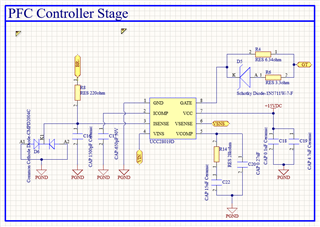
After this test, no physical error appeared, and D6 diode was canceled because it did not have any effect on the Isense pin other than protection, and D7 diode was also canceled because it had a protection function. However, because we missed it, it was forgotten to connect the R8 pin, which provides the connection to the Isense pin, to the system. In other words, the current information to the integrated is blocked unintentionally. After these corrections, the system was connected to the mains again. It has been observed that fume comes out of the TPS5431 integrated, which feeds the UCC28019.

After the last test, all systems and components were checked for short circuit. As a result of this control, the R8 resistor was jumped with a copper cable and the Isense pin was included in the system by connecting the continuation of R13 with the BR- pin of the C3 capacitor. It was seen that the "VIN" and "ENA" pins of the TPS5431 IC were short-circuited and replaced with a new one. Afterwards, it was observed that the legs of the Q1 MOSFET were short-circuited. It was removed from the circuit and after the internal diode and internal resistance control performed outside, it was determined that it was broken and replaced with a new one. In the continuation of the controls, although a capacitor was connected to the Icomp pin of the UCC28019 IC, it was observed that the pin was short-circuited directly to the ground (GND pin) and it was determined that the UCC28019 was broken and replaced with a new one. After all these changes, short circuit control was made with reference to the design images given above and the system was connected to the network for the third time.

In this test, the mains connection was disconnected with the arc sound coming from the system. In other words, the network connection time of the system is maximum 1 second. In the controls made after this test, it was observed that the Icomp pin of the UCC28019 was short-circuited to GND and the "VIN" and "ENA" pins of the TPS5431 were short-circuited. No physical damage was observed on the elements in the visual inspection made after this test. It has been observed that the control of the Q1 MOSFET is robust. However, the UCC28019 and TPS5431 ICs are damaged.

Questions:


  1. Could the problems be caused by programming the Vcomp and Icomp pins with wrong values?
  2. Could the problems occur because the boost coil value is too high than the minimum value?
  3. Could the problems be caused by the irregularities of the boost coil in my own winding?
  4. If you think that the problems are caused by the pcb, I can send the design files via DM.
  5. Other than these possibilities, I have difficulty in estimating the source of the problems. I would be glad if you help.
  • Hello Cihangir,

    There's nothing in your design that stands out as an issue.  The Vcomp or Icomp setting settings wouldn't cause this type of issue.

    Your inductor has only 15 turns for 0.6mH, so I am curious what core material you are using. It's very possible that the inductor is saturating very quickly causing your problems.

    To protect your circuit while debugging, it may help to increase your thermistor to 10Ω.

    Regards,

    Ray

  • Hello Ray,

    Thank you for your response. I will change the thermistor to 10 ohms.
    The core material of the coil is CF139. The inductance factor is 2600 nH. I have a lack of information about the saturation of the coil, I would be happy if you inform me about this issue. How can I calculate about this subject while designing the coil?

    Kind regards.

    Cihangir

  • Hi Cihangir,

    Manganese-Zinc alloy is used in ferrite cores. What you have is a gap-less ferrite and not really the inductor that you are expecting at these currents. A ferrite will saturate almost immediately. For example, flux density = LI/NA. Assuming a peak inductor current of ~10A and a core cross-sectional area of ~100mm^2, your inductor would require a flux density of at least (600 * 10)/(15 * 100) = 4T . The core material you have has only 0.49T

    If you'd like to learn more about magnetics, TI has a book on magnetics design: http://www.ti.com/lit/slup132

    Maybe you can get the same inductor used in TIDA-010080 (Wurth electronics, part number 750344651)

    Regards,

    Ray

  • Hi Ray,

    Thank you for your responses. I checked the coils I have and found a coil with digikey part number "1140-471K-RC". The current limit of the coil is 4.9 A and the saturation current is 9.5 A. In the black box calculations of the circuit I told you about, the input voltage range is defined as 90 VAC-265VAC. I currently do not have a coil to meet these ranges. However, I am testing the circuit with 220 V AC. At this voltage value, I can calculate 700 W/220V=3.18 A, I_in_max=4.49 A, I_ripple=1.79 A, I_L_peak_max=5.38 A, current values. Theoretically, I don't see a problem with these accounts. Do you think the coil will cause problems again?

    Kind regards
    Cihangir

  • Hi Cihangir,,

    That coil is still a ferrite core, but according to the specs, it should be better than the one you were using.  Before you begin, make sure you've replaced all of the suspected damaged components and start with a very light load.

    Regards,

    Ray

  • Hi Ray,

    I experimented with the coil I mentioned in my last post. In the schematics seen in the above articles, the R8 resistor (0.25 W) connected to the Icomp pin burned out. After connecting the circuit to the mains, about 6 seconds later, an arc occurred in the area where R8 was and I cut the connection. However, the Icomp pin of the UCC28019 IC was short-circuited to the GND line, and the VIN and ENA pins of the TPS IC were short-circuited. There was no load connected to the system at the time of the test. The MOSFET is solid. In addition, the bulk capacitors at the PFC output were charged up to 30 V. I can't understand what the problem is. I would be glad if you help.

    Kind regards
    Cihangir.

  • Hi Cihangir,

    First, I think you mean R8 connected to the ISENSE pin.  For this resistor to burn out would mean there was >7V across it.  I can't see how that could happen under normal conditions.

    That said, I was focusing on the PFC circuit since I support the UCC28019, but I think the issue is likely with your 15V supply. I looked at the datasheet for the TPS5431 and the first thing I noticed was that the AbsMax is 25V for VCC and 7V for EN; I'm pretty sure you're violating those.  Take a step back and disconnect your 15V supply (remove L6) and use an external supply to power that net.  Obviously, you need to replace the UCC28019 since the ICOMP (or ISENSE) pin is shorted to GND.

    If that works, you'll need to work on the DC supply (remove the UCC28019 while you're doing this).

    For when things get running, you'll probably want to decrease C3 to ~0.22uF. 1uF may result in relatively high distortion at the zero crossover points.

    Ray

  • Hi Ray,

    The transformer I use on the 15 V supply stage converts 230 VAC to 12 VAC. However, before testing the PFC stage of the circuit, I tested the 15V supply stage separately and it was working fine. I would appreciate if you explain why you think I exceeded the maximum values.

    You are correct in your advice about the C3 capacitor. On my last try, I lowered it to 0.56 uF and did my test.

    What are the chances that these problems I'm experiencing are caused by the PCB design? The burning of my integrated circuits in every attempt started to force me financially.

    Kind regards
    Cihangir

  • Hi Cihangir,

    OK, no issue with violating AbsMax on the 15V supply. I missed that the transformer wasn't 1:1.  However, you do need to understand why the VIN and ENA pins of the TPS IC were short-circuited; they are input pins so nothing "downstream" should be able to affect them like that.

    It's pretty clear that the issue you're experiencing isn't a "PFC" issue but rather some other circuit or setup problem. Because you're not able to get PFC regulation, it's difficult for me to help you much until you get past this issue.

    At this point, there are two main areas that you need to consider:

    1) Isolated source:

    • Are you using a completely isolated AC source?
    • Are you certain you're not creating unintended ground connection(s) with your scope probe grounds?

    2) Physical board:

    • Does your layout match the schematic?
    • Is there a board build issue where the layout does not match the schematic?
    • Is there some other error in the layout?

    I recommend you start simply with and undamaged setup and check connections and values with a multimeter.  If all checks out, add circuitry one small block at a time and make sure the voltages are what you expect at each step before continuing on to the next. Pay special attention to your grounding and isolation along the way.

    Ray

  • Hi Ray,

    I fixed the problems. Currently, I do not get any error while the system is fed from the mains and the pfc integrated is fed. But the system does not boost. In my last attempt, my IC is supplied with 14.6 V and I saw 12 V on the gate pin. My output voltage is measured as 328.1 V. I did the calculations specified in the datasheet for output voltage stabilization. What do you think is the source of the problem? Could the voltage falling on the Vın pin and the voltages falling on the Vsense pin have protected the system? The current output voltage drops to the Vsense pin is 4.2 V. According to the data sheet this should put the system in undervoltage protection.

    Kind regards
    Cihangir

  • Hi Cihangir,

    I'm glad to hear you've gotten through your previous issue. It now sounds like you're getting some PFC fault causing it to stop sending gate pulses.

    Since you don't seem to get any PFC/Boost regulation at all, you need to probe the signals during startup (as you apply the line voltage).  Look at VINS, GATE, VSENSE & IL1 to check if you're getting an output over current or over voltage faults. Zoom in to the area around when the GATE pulses stop. If you don't find the issue there, then monitor GATE along with VCC, VCOMP and ISENSE.

    Ray

  • Hi Ray,

    Thank you for your suggestions. But it may take some time for me to prepare an isolated oscilloscope. Can you make a suggestion based on the schematic I sent you until I get this done?

    Kind regards
    Cihangir

  • Hi Cihangir,

    Nothing stands out from your schematic.  The output capacitance is pretty high and the compensation is a bit aggressive (C22 can probably come down by an order of magnitude), but I don't see either resulting in the output not coming up.

    For now, you can skip the input supply signal for now and just focus on the other signals. They can all be referenced to PGND.

    Regards,

    Ray

  • Hi Ray,

    I measured the voltages falling on the pins. I have listed the data below. I have attached the oscilloscope image of the Gate signal. What do you suggest I do ?

    Vcomp: 7.4V
    Vsense: 4.1V
    Vcc: 14.7V
    Gate: 12V
    Icomp: 1.1V
    Vins: 4.2V
    Isense: 0V
    Vout: 326.7

    Kind regards
    Cihangir

  • Hi Cihangir,

    I apologize for the delay. I noticed you opened up a new thread, I will close that as they all get assigned to me anyway :).

    If you notice, your COMP voltage is maxed out (in fact, it is exceeding the 7V AbsMax spec!). Your gate on-time is maxed out and VSENSE is on the high end. The PFC has likely hit it's OCP level and you are peak-regulating (√2 * 230Vac + Vdiode = 326V).

    As requested a few days ago, please provide IL1 during startup so we can see what your actual inductor current is.  Do this with no load so you can get a baseline.

    Thank you,

    Ray

  • Hi Ray,

    I solved the problem. I reduced the number of bulk capacitors at the output to two. I'm still above the minimum required capacitor rating. And when you do that, boost is turned on. I saw 390VDC. I attribute the reason why Boost is not active because the capacitors are trying to charge at the start. There may be a different reason, but doing this solved the problem. Your comment is also important.

    When I solved this problem, I should have installed the PFC, but since I did not have the load, I soldered the remaining parts to try my next stage, LLC, without load. I am powering the system externally with an external PSU. After connecting the system to the grid, I give the supply voltage to the integrated circuits. When I connected my full circuit (PFC+LLC) to the grid with the same procedure, my mosfet in the PFC and then my shunt resistor burned out. I couldn't understand why the part that worked before gave such a result even though I had activated the integration yet.

    I am using UCC256402DDBRCT as LLC IC. A different integration has been included in the title, should I open a new topic?

    Kind regards,
    Cihangir

  • I believe what you are saying is that now your circuit with the PFC alone boosted properly to 390V without a load but you did not test it with a load. Then, when you connected the LLC (still with no load), the MOSFET and sense resistor were damaged. If that is the case, then yes, open a new thread with UCC256402DDBRCT in the topic. However, if the issue is simply due to the addition of a load, I suggest you disconnect the LLC again get the PFC regulating again with no load and then add a resistive load (power resistor or light bulb(s) can be used). Start with a small load current, and monitor IL1 at startup.

    Regards,

    Ray