Hello,
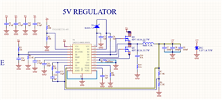
I currently use the LM25116MH in our designs extensively as our DC/DC buck converters.
We use 2x 6S LiPo batteries (nominal 24V, max is 26V fully charged each with 4500mAh capacity) as our power source and we use this controller to step-down to 5V nominal.
For this particular design for which I am having issues with, we actually had designed this buck converter to output 5V with a max of 7A on a previous revision and it worked perfectly fine (i.e. heat dissipation was nominal and handled well, and good line regulation)
Due to issues with an on-board USB hub controller, we found that filtering the buck converter with an RC circuit and some value changes reduced the ringing that we suspected was causing our USB issues.
We created a new revision a few days ago trying to incorporate the changes and make PCB layout changes that were more closely following the evaluation board layout.
Another notable change is the SW copper area which is much less than before with no real thermal vias for dissipation other than through the MOSFET pad themselves. I read an article for how to reduce power supply noise and one thing that was mentioned was to reduce the SW node copper area.
When we first turned it on with about a 2A load on the 5V line, the inductor heats up significantly almost immediately. About a minute of operation, the inductor starts audibly ringing. In less than 2 minute, the inductor gets to about 125degC and eventually shuts the 5V line down.
Since that issue, I have updated the error compensation network to match the WEBENCH results and used another inductor which has a higher current rating but the same inductance value, but still see the same results.
I was wondering if anyone can help guide me into rectifying this issue? Measurements that might be useful to know or anything else.
I have attached a screenshot of the schematic and a PDF of the PCB layout. The only values in the schematic that have changed are the error compensation network components, all other component values match the schematic below.
For the PCB:
Top Layer - GND Plane
Inner Layer 1 - GND Plane
Inner Layer 2 - Power Plane
Bottom Layer - GND Plane


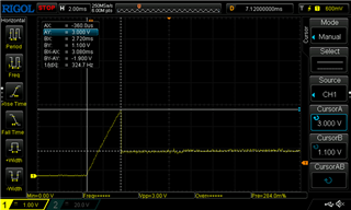
 This is the SS pin
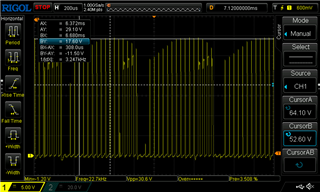
 This is the SW node on the controller
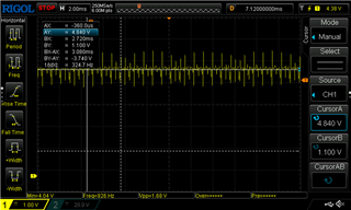
 This is the UVLO pin