This thread has been locked.

If you have a related question, please click the "Ask a related question" button in the top right corner. The newly created question will be automatically linked to this question.

TPS552882-Q1: The internal switching frequency is not meet FSW resistor setting.

Part Number: TPS552882-Q1

Hi Sir,

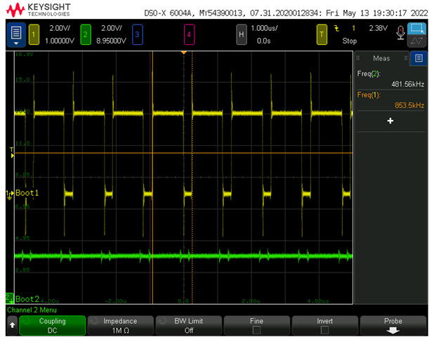
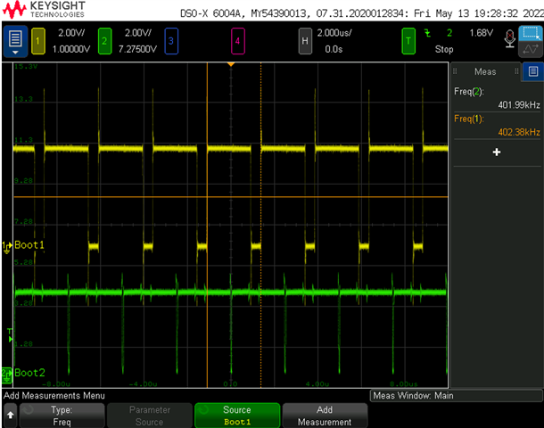
    The TPS552882-Q1 which switching frequency is not meet our setting by resistor. 

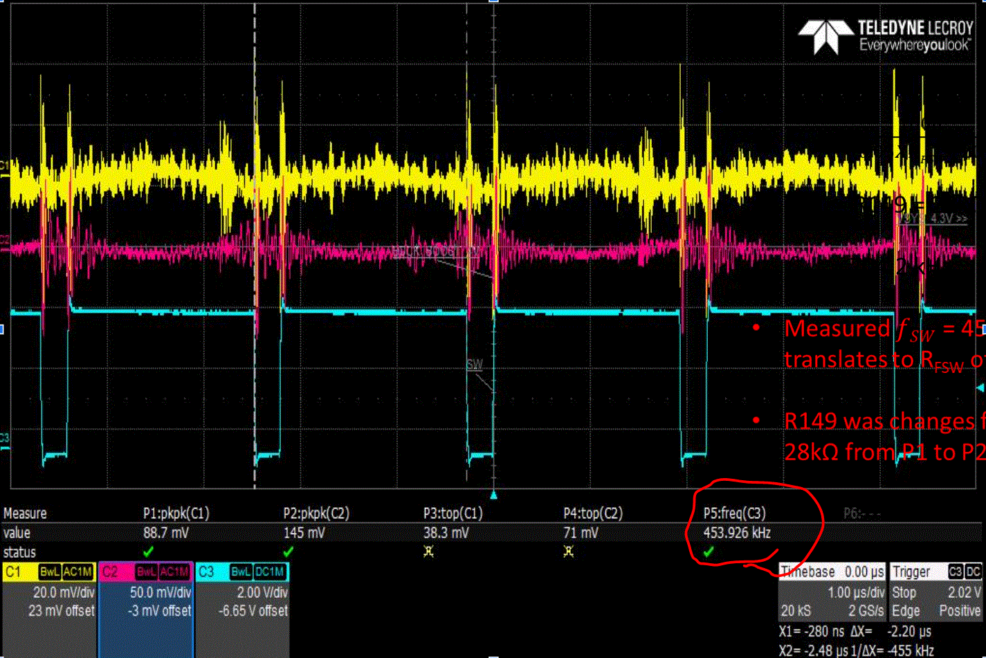
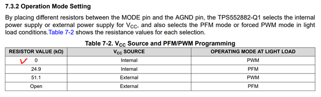
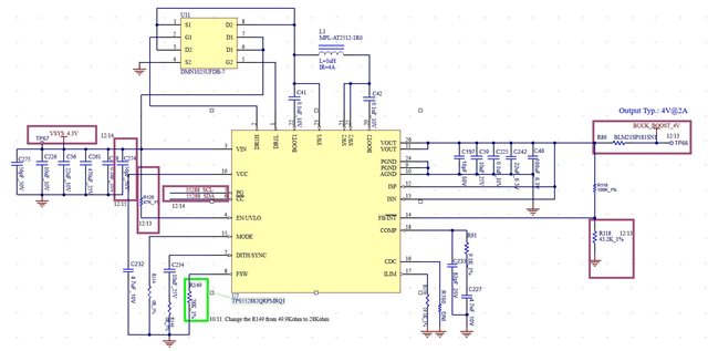
We set the internal Vcc source and PWM mode on the TPS552882-Q1. And we connect the FSW pin to 28kohm and tie it to the ground. 

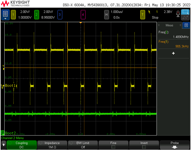
So that means the internal clock will be 704.2khz, but we measured the internal clock frequency only 453.9khz.

I have attached the our schematic and the measurement waveform.  Could you help clarify the root cause?  

  • Hi Godfrey,

    What's the input voltage now? Could you increase the Vin to above 5.5V and test the switching frequency again?

  • Hi Zack,

            The input voltage is 4.3V, our power architecture won't use input voltage over 5.5V to this buck-boost converter. So I am wondering know why the switching frequency is related to the input voltage? And I thought the TPS552882-Q1which min input could support to 2.7V, the switching frequency should not impact from input voltage. 

  • Hi Godfrey,

    The reason is when Vin is close to Vout, the device works in buck-boost mode with all four FETs switching at half setting fsw. When Vin is larger than Vout with certain voltage, it goes to buck mode and switching frequency is set by Fsw pin resistor.

    So you can check if the switching frequency is correct in buck mode.

  • Hi Zack,

        After increasing the input voltage to 5.1V or 5.2V, I could measure the higher frequency close to our setting on BOOT1.

    And why I can't measure the switching waveform on BOOT2 at the same time? When I set the input voltage on 4.3V, I could measure the waveform on BOOT1 and BOOT2 at the same time.

    Input 5.1V output 4V

    Input 5.1V output 4V

    Input 4.3V output 4V

  • Hi Godfrey,

    When VIn is higher than Vout at certain level, the device works in Buck mode. The internal High side FET is always on, so SW2 voltage = Vout voltage. SW1 is switching.

    When Vin is less than Vout at certain level, the device works in boost mode, the external high side FET is always on, so SW1 voltage = Vin voltage. SW2 is switching.

    When Vin is close to Vout, all four FETs are switching, both SW1, SW2 are switching.

  • Hi Zack,

     Got it, mostly the input will be 4.3V close to the output 4V for our power design. Is it okay to continue running all four FETs switching at all times in the current power design? Any risk we need to be notice? 

  • Hi Godfrey,

    There is no risk to let all four FETs switching at all times in this design. You can share the layout so that we can double check it.