This thread has been locked.

If you have a related question, please click the "Ask a related question" button in the top right corner. The newly created question will be automatically linked to this question.

LMG3422R050: Datasheet clarifications of turn on loss, diode conduction loss

Part Number: LMG3422R050
Other Parts Discussed in Thread: LMG3425R050

Hi Experts!

I am creating a PLECS model for this device. I have a few questions on the LMG3425R050 datasheet, which will help me make this model more accurate.

1) For graph 7-11, what temperature is this? Is it safe to assume this graph is true across temp spec -40C to 150C?

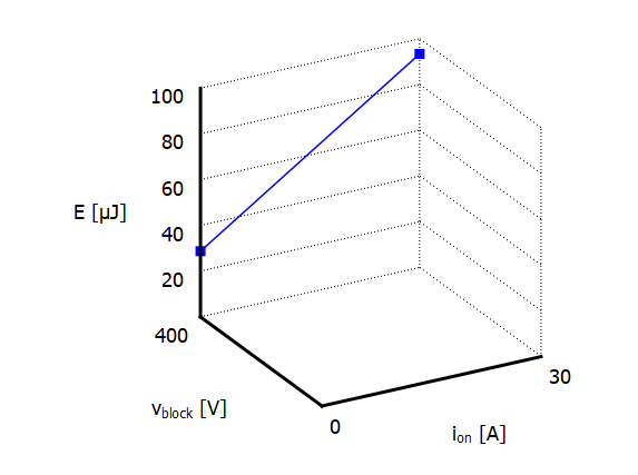
2) For graph 7-11, what is the blocking voltage? In my PLECS model, turn-on and turn off losses are a function of i_on and V_block:

3) Could you please explain what graph 7-6 shows? I believe it is the body diode conduction loss, but I may misunderstand.

Thank you!

  • Hi Cameron,

    1. This plot is at 25C. 

    2. These switching energy data are taken at V_block of 400V. 

    3. This is the Voltage drop across Source and Drain of the device Vs source current when IN signal is low (when device is switched off). Please note that this is only for LMG3422R0x0 (without operational ideal diode mode). In LMG3425R0x0, there is a feature called Operational ideal diode mode, which reduces the off-state third quadrant losses by enabling the switch. You can refer to section 9.3.10 for more details.

    With Regards,

    Prasanna U R