Because of the holidays, TI E2E™ design support forum responses will be delayed from Dec. 25 through Jan. 2. Thank you for your patience.

This thread has been locked.

If you have a related question, please click the "Ask a related question" button in the top right corner. The newly created question will be automatically linked to this question.

TPS61032: Design review of circuit and layout

Part Number: TPS61032

I'm using the TPS61032PWPR in a new design. Input:
5V DC after diode V drop: 4.5-4.8V
Battery: 3.0-4.2V
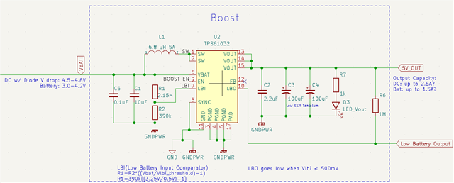
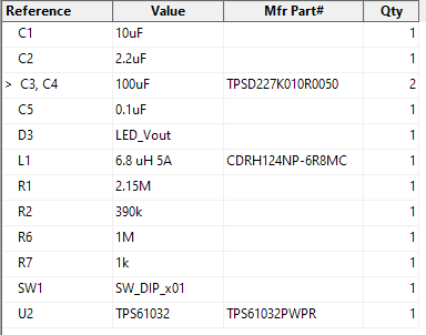
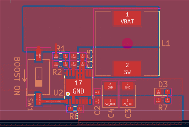


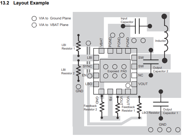
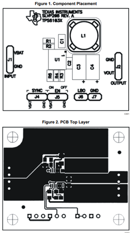
Since I'm using the TSSOP package the layout is based closely on the TPS6103x EVM-208 datasheet in addition to the TPS61032 datasheet. I'm looking for general feedback on the schematic and layout, and I have a few questions as well:

1: The layout example in the TPS61032 part datasheet shows many vias to ground (by the input and output caps, in the thermal pad, and by LBI resistor 2).  but the evaluation module layout just has 1 via to ground near pin 9.  Which method is preferred?
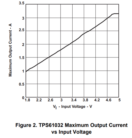
2: Based on my inputs (DC 4.5-4.8V and Bat 3.0-4.2V) and Figure 2 of the datasheet. It seems that I should be able to get at least 2.5A+ when using the DC supply, and 1.5A+ while using the battery supply. Can this graph be taken at face value or are there other considerations that limit the output current?


  • Hi Rich,

    For your two questions:

    1. Thermal pad vias should not be too few, otherwise there will be some problems with chip heat dissipation. The vias to ground by output capacitors are also important to reduce switching loop impendence. The other vias are not so critical.

    2. What Figure2  shows is maximum output current vs. input voltage, not minimum current. For example, the point (4.6V, 3A) means that output current can range from 0A to 3A when input voltage is 4.6V. 

    Best Regards,

    Nathan

  • Hi Rich,

    Thanks for reaching out. Below are some comments on the schematic and layout:

    1. What is the maximum output current of the device?

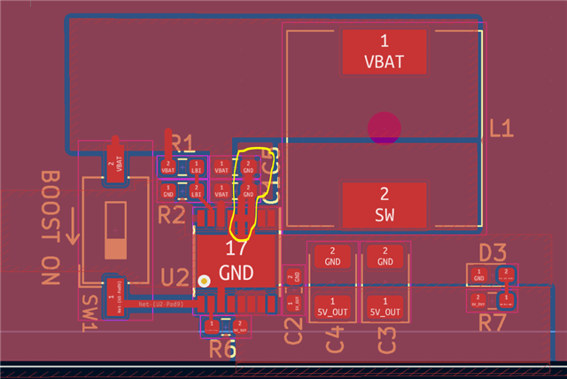
    2. Pour the solid copper region but not the crossed copper in the yellow region.

    3. Swap the position of C1 and C5 to put the 0.1uF(C5) near the Vin pin.

    Regards,

    Bryce


  • Thanks for your feedback:
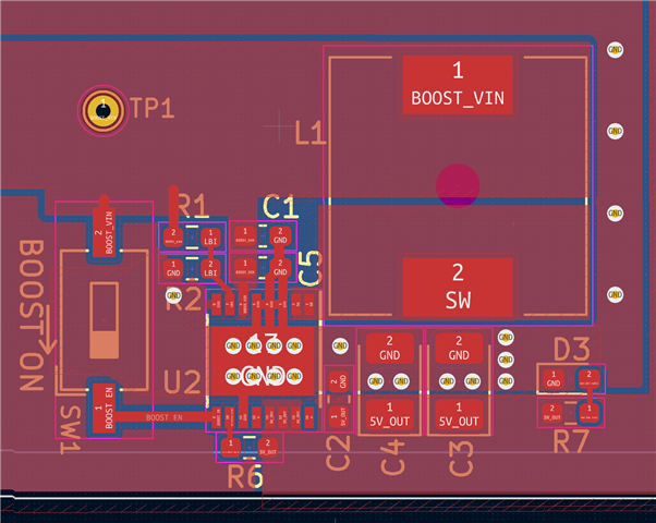
    1: I added via mainly on the thermal pad and by the output capacitors. (see image below)
    2: Yes, that is my understanding, that Figure 2 shows the maximum output current at a given input voltage.

    @bryce xun
    Thanks for your feedback as well:
    1: The maximum input for the target device's PMIC is 2.5A @ 5V.  In tests so far current consumption has only been in the 500-750mA range,  but the firmware has not been finalized so I'm looking to understand how current it will be capable of delivering.  The numbers I quoted were based on Figure 2 staying below the max current.
    2: I added a keep out to eliminate the ground pour in the area you highlighted.
    3: I swapped C1 and C5 to get the 0.1uF cap closest to Vin

    Let me know if there are any other recommendations after making the suggested adjustments.

  • Hi Rich,

    1. You are right. The maximum output current capability depends on your input voltage (DC 4.5-4.8V and Bat 3.0-4.2V).

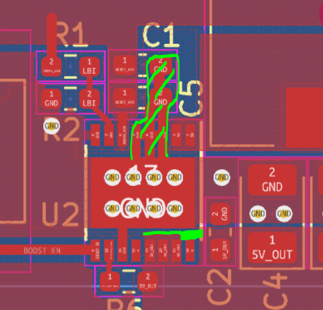
    2. Maybe you have mistaken my words, what I mean is that you can pour the GND with a full filled copper plane like below, but not the crossed copper.

    3. It will be better if you can make the route from Vout pin to Cap pad like below so that the switching loop would be smaller.

    Regards,

    Bryce