This thread has been locked.

If you have a related question, please click the "Ask a related question" button in the top right corner. The newly created question will be automatically linked to this question.

TPS650861: Transient response issue

Part Number: TPS650861

Hi, 

In the design we use TPS650861 to power up NXP LS1046 processor. 

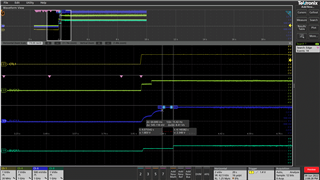
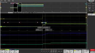
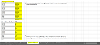
Power sequencing is as follows : CTL1 will power up Buck3> Buck 4> Buck 1 >LDOA3 CTL2> Buck 2 and CTL3 >Buck6. 

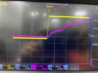
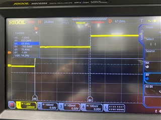
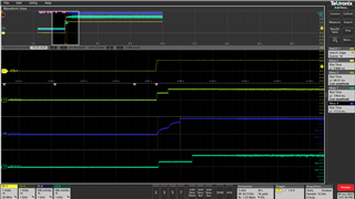
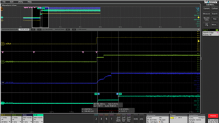
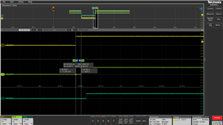
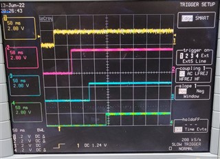
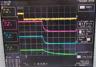
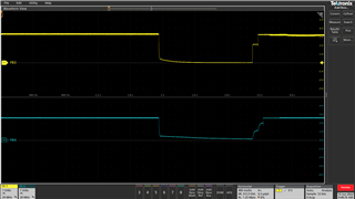
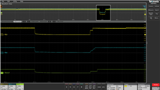
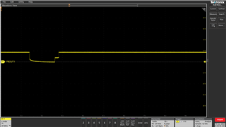
We are facing issue with transient response of Buck regulators(4,3,1) in CTL1 sequence.

Buck 3 is the first rail powered on. Buck 4  rail is sequenced based on CTL1 and PWR good of Buck3 . Buck 1 is sequenced based on CTL1 and PWR good of Buck 4.

Ramp up is not smooth for all the 3 rails. OTP programmed for DVS enable, Step size of 25mV and  Rise time delay of 64ms.

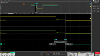
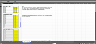
Attached the OTP generator sheet and Waveform capture for Buck 3 and Buck 4 .

CTL2 and CTL3 voltage rails are fine. Is there a way to improve the transient response . Please advise.

PMIC OTP.xlsx

  • Hi Divya,

    Could you provide a PDF copy of your schematic? I can set up a direct message with you if you need to share the document privately.

    There are a couple additional scope captures I would like to see as well:

    • Could you provide a scope capture of VSYS, LDO5P0, CTL1, and BUCK3 all in one picture. Please show the rising edge of all waveforms if possible. I would like to see the timing of each signal.
    • Could you also provide a scope capture of CTL1, BUCK3, BUCK4, and BUCK1 all in one picture. Please show the rising edge of these waveforms as well so I can look at the timing.

    Double check the Schematic Checklist for the TPS650861 device and make sure all the necessary external components are placed. Once I see the schematic I can provide a more detailed analysis.

    Regards,

    James

  • Hello James,

    Could you please drop me a direct note on my email id so that I could share the details with you.

    Thanks,

    Divya

  • Hi Divya,

    Please accept the friend request I just sent you. Once you accept the request, you can mouse over my name here on the forums and select "Send Private Message". You can also do this from your profile friends list.

    Regards,

    James

  • Hi Divya,

    I have a large amount of support requests at the moment but I will update this thread with my advice within the next 2 business days.

    Regards,

    James

  • Hi Divya,

    While I'm taking a look at the schematic can you provide those scope captures? I'll repost them again below:

    • Could you provide a scope capture of VSYS, LDO5P0, CTL1, and BUCK3 all in one picture. Please show the rising edge of all waveforms if possible. I would like to see the timing of each signal.
    • Could you also provide a scope capture of CTL1, BUCK3, BUCK4, and BUCK1 all in one picture. Please show the rising edge of these waveforms as well so I can look at the timing.

    Regards,

    James

  • Hi Divya,

    After looking at the schematic, here is my feedback:

    • For PVINLDOA2_A3, we recommend a 4.7uF ceramic capacitor and it looks like you have a 47uF capacitor currently placed. This might be related to your issue with the transient response as this is 10 times the recommended value of capacitance.
    • The resistors on FBVOUT2 and FBGND2 say "DNP". If you have the connection closed by some other components then that is fine.
    • Make sure CTL1 is not pulled high to early in the power sequence. Without the scope captures showing the timing of VSYS, LDO5P0, CTL1, and BUCK3 it is hard for me to tell how the sequence looks overall. CTL1 should only be pulled high once VSYS and LDO5P0 are both stable.
    • Double check the equations for the inductors, output capacitors, and ILIMx resistors for the problematic rails. The components you have seem fine to me but this can be a safe precaution.

    Regards,

    James

  • Hello James,

    Thanks for the reply.

    We tried with 4.7uf for PVINLDOA2_A3. Transient response did not improve.

    The resistors on FBVOUT2 and FBGND2 is populated.

    CTL1 is high once VSYS and LDO5P0 is stable.

    Please find attached power rails waveforms attached. Please review and feedback.

    Thanks,

    Divya

  • Hi Divya,

    Can you try disconnecting all loads from the PMIC and testing the buck outputs again? Do the waveforms look the same? (Let me know if these scope captures were taken without a load already).

    Do you have another TPS650861 device you can test? Do you see the same issues on other devices or only one device?

    BUCK4 should not be activating until BUCK3 PGOOD is asserted. The BUCK3 PGOOD should not be asserted until the rail is at the correct voltage level. Right now I see BUCK4 is ramping up before BUCK3 reaches the target 3.3V. That transient response is abnormal but I believe the more important issue may be the fact that the device is not responding to PGOOD logic correctly. The behavior on BUCK3 should be causing a power fault in the device. If a power rail fails to reach the target VOUT within ~10ms the device should issue a reset and a new power cycle should start. This picture is from the datasheet:

    Regards,

    James

  • Hello James,

    The waveforms shared are with load connected. I dont have option to disconnect load in the custom board.

    I checked in TI evaluation board without load .PFA snapshot of Power up and power down sequence in TI evaluation board.

    For Power down sequence, step response is observed in evaluation board . Looks different from datasheet specs.

    We observed same response in all 3 boards we tested. PGOOD may not be behaving the right way However first Buck regulator from CTRL is showing a step response. The first rail does not depend on any PGOOD. 

    Power rails are stable after power up. We assume no power faults are generated. I am checking on optimizing the output caps and also trying with adjusting the rise time.

    Please share your thoughts on this.

    Thanks,

    Divya

  • Hi Divya,

    The power up waveforms look cleaner on the EVM so there may be an issue with the way the PMIC interacts with the load on your custom board. 

    As for the power down behavior, I took another look at your OTP and I noticed that all the power rails are set to "No Discharge" in the Additional Details tab of the OTP generator. Try changing all the rails to 100 Ohms so that the power rails discharge predictably. This issue may not have been apparent with your custom board because the load would pull the excess charge from the device during power down.

    I loaded your OTP settings onto an evaluation module and ran some of my own tests. I had the 100 Ohm discharge enabled during these tests:

    OTP Generator with 100 Ohm discharge resistance enabled for all rails (try changing this in your OTP)

    Power up sequence of CTL1 (YELLOW) > BUCK3 (RED) > BUCK4 (BLUE) > BUCK1 (GREEN)

    Power down sequence of CTL1 (YELLOW) > BUCK3 (RED) > BUCK4 (BLUE) > BUCK1 (GREEN)

    If you take more measurements of the waveforms from your custom board, could you share some scope captures of FB3, FB4. and FBVOUT1 pins? I would like to see what the bucks are receiving from the output during the strange transient behavior.

    Regards,

    James

  • Hello James,

    PFA waveforms from custom board for FB3, FB4, FBOUT pins.

    Thanks,

    Divya

  • Hi Divya,

    Thank you for sharing those scope captures.

    My current theory is that you need to have the discharge resistors enabled in the OTP settings so that charge does not build up on the buck outputs before the power rails are supposed to ramp up. Currently, you have BUCK3, BUCK4, and BUCK1 set with a 64ms delay timer. In the scope captures we can see that the bucks ramp directly to their target voltage AFTER the 64ms timer on each rail expires. All of the unexpected transient behavior occurs before the 64ms timer is finished on each rail. I don't think the PMIC checks for power faults until the delay timer is done and the buck is allowed to ramp up using DVS. This would explain why no reset signal is issued for the strange transient behavior.

    As an additional check, I opened up the OTP Generator document we provide for the NXP L1043 which is from the same processor family as your device. If you look at the "Additional Details" tab, you can see that the recommended settings are for all power rails to have discharge resistance of 100 Ohms set up:

    I would recommend you change all the power rails to 100 Ohm discharge resistors in your OTP. If you have a way to hold the CTL1 signal low after VSYS and LDO5P0 ramp up to a stable voltage, you can change the value of the DISCHCTRL1 register (R = 0x40) to a value of 0x51 and write the register. This will enable the 100 Ohm discharge resistors on BUCK3, BUCK4, and BUCK1. This should be good enough for a quick test.

    From there you can pull CTL1 high and see if the new OTP setting fixed the transient issue. This method allows you to test the fix without having to burn in a new OTP memory bank. However, this is only possible if you can hold CTL1 low during the manual programming process while you change DISCHCTRL1.

    If you cannot hold CTL1 low, you will need to burn the updated settings into memory bank 1 on the PMIC since this is a power up issue. Any time the device is power cycled, it will revert to the default programmed settings so any changes to the DISCHCTRL1 register will be lost.

    Regards,

    James

  • Hi Divya,

    An additional note for you:

    Since the power up waveforms from your EVM testing were clean and did not show the abnormal transient behavior, you may have an issue with leakage from the processor. The timing of the voltage response on BUCK4 falls in line with the step responses on BUCK3 and BUCK1.

    Such testing would need to be done by removing the processor or otherwise disconnecting the PMIC from the load system. If this cannot be done then it will be difficult to find the source of the issue.

    Beyond changing the discharge resistor settings and testing the PMIC without the processor load, you can try reducing the 64ms delay times. Most processors do not require such long delay times on all of the rails.

    Regards,

    James