This thread has been locked.

If you have a related question, please click the "Ask a related question" button in the top right corner. The newly created question will be automatically linked to this question.

LM51561H: External clock spec inquiry from LM51561H

Part Number: LM51561H
Other Parts Discussed in Thread: LM51561, LM3488

I want to use the external clock synchronization function on the LM51561.
External clock is planned to be made in FPGA, 3.3V level, 120KHz.
Please refer to Figure 1 below for details.
The specification of the required external clock could not be found in the datasheet.

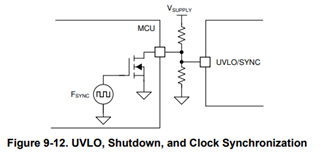
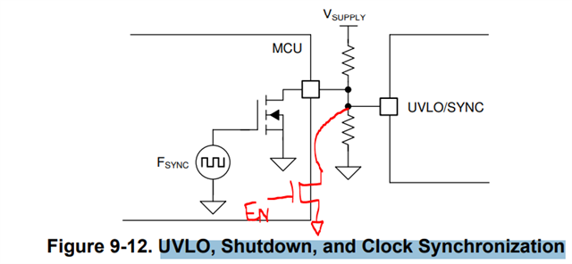
There are electrical properties related to UVLO/SYNC on page 6 of the datasheet, but I don't quite understand.

The working scenario is as follows.
When the system boots for the first time, it operates with the RT-set resistance value, and when the FPGA is downloaded and initialized, the FPGA will provide an external clock.

I ask you three questions below.
1. Inquire about synchronization signal threshold specifications (High level, Low level).
2. In Figure 1 below, I ask if there is any problem even if you use it like R13 and C19.
3. If you can use it like R13 and C19 in Figure 1 below, please inquire about the formula to set the R/C value.

4. If there is a better way, please suggest.

For reference, the example below is an example of the external clock spec in the LM3488 data sheet.

  • Hi Honggyo,

    The engineer responsible for this part is currently out of office and will be back by next week. But for now, you may consider the following:

    The specifications are provided in the datasheet in section 9.3.6. The main criteria here is that the UVLO pin should be pulled below 1.45V with the minimum pull-down pulse width greater than 150ns, and minimum pull-up pulse width greater than 250ns.

    Generally, the SYNC is implemented with an open-drain output of the MCU pulling down the UVLO pin, so the RC network may not be required. 

    Regards,

    Richard

  • Hi Richard

    Thanks for your quick reply.
    These are three of my questions.
    I saw datasheet 9.3.6 as well.
    However, information about the high level and low level of the sync clock is not available.
    please check.

    Best Regards

    Lee honggyo

  • Hi Honggyo,

    this parameters are shown here:

    Best regards,

     Stefan

  • Hi Stefan,

    Thank you for answer
    I hope you have a good look at my whole question.
    I am inquiring about 4 items.
    Please review the circuit configuration in Fig.1.
    i.e. I try to use both EN/UVLO/SYNC functions.
    And when I briefly mention the answer you gave, I also said in the question description section, "There is an explanation on page 6 of the data sheet, but I don't understand it well." Below is the part I understood after looking at the datasheet.
    Is my understanding correct?
    High-level input voltage(min) = 1.575V ?
    Low-level input voltage(max) = 1.370V ?
    Recommended amplitude > 0.2vpp ?
    Thanks for the quick review.
    Please review the circuit configuration in Fig.1 (use all EN/UVLO/SYNC functions).
    thank you

    Best regards,

    HongGyo

  • Hello, 

    Thanks for reaching out. We might suggest using the same configuration as in figure 9-12 (basically adding a MOSFET) instead of  R19 and C13 keeping M1 like in your schematic: 

    Yes, those you indicated are the thresholds. Please let us know if you need further help. 

    Kind regards,
    EM 

  • Hello EM,
    Thank you for your comments.
    Figures 9-12 were reviewed early in the design.
    However, when UVLO is set, the pull-up resistance becomes large.
    In that case, the rising time of the external clock is greatly increased.
    The figure below is the result of my simulation.


    If you reduce the pull-up resistance of setting UVLO, the clock rising time is improved, but
    The current consumption of 17V will increase significantly.
    In simulation, you need to set the pull-up resistance of UVLO setting to 5K or less to see improvement in clock rising time.
    So my review was to either use a buffer or use serial R/C.
    1. When using a buffer, the concerns are as follows.
    If the pull-down resistor 10K at the bottom of the UVLO setting is not properly soldered on the reflow, 17V will be applied to the buffer output. In this case, there is a concern that the buffer may be damaged by over voltage.
    What should I do? Is this a useless worry?
    2. When using serial R/C, the concerns are as follows.
    If the lower pull-down resistor 10K is not properly soldered on the reflow, it works without any problem.
    However, the shape of the clock changes slightly.
    Of course it's much better than driving it with a FET.

    Best regards,

    HongGyo

  • Hello HongGyo,

    Please explain which problem you have with the increase rise time of the external clock signal. The moment when you get above the threshold is slightly shifted, but as this is the case for all rising edges, I wonder if this is really a problem. The clock is synchronized on the falling edge.

    1. Yes, if you are using a buffer that does not have an output which can handle the maximum input voltage on the P17V line, you might damage it in your scenario. You can reduce the likelyhood of this to happen by splitting the lower resistor into 2 pieces in parallel that limits the voltage if just one is not soldered.

    2. I did not test if synchronization works properly with the RC network you want to use. You could order an EVM and check it out.

    Best regards,
    Brigitte