This thread has been locked.

If you have a related question, please click the "Ask a related question" button in the top right corner. The newly created question will be automatically linked to this question.

LM5164-Q1: LM5164

Part Number: LM5164-Q1
Other Parts Discussed in Thread: LM5164

Hi sir,

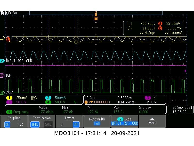
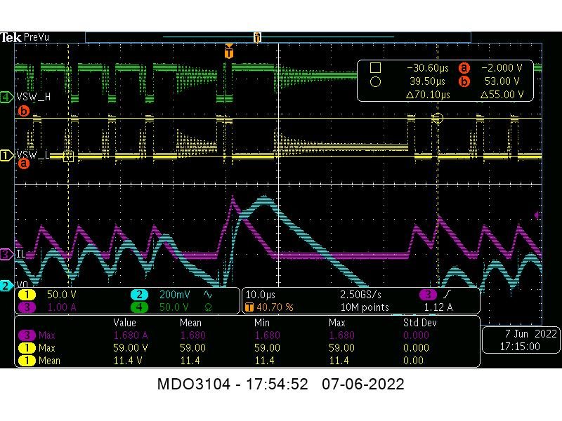
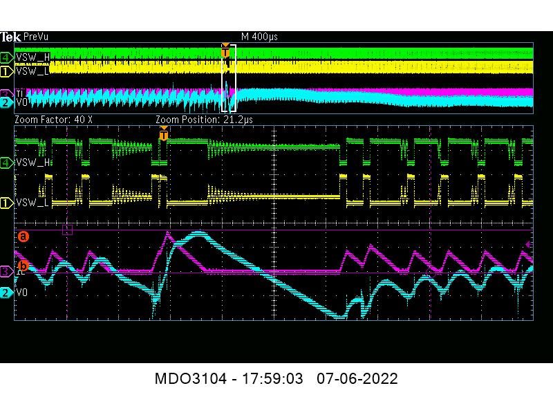
We are using LM5164-Q1 converter  for step down application from 56 to 12V for driving load 630mA load.

We are used L-C filter combination for reduce ripple from input supply and reject unwanted noise also.

But we also kept reverse blocking diode in series before L-C filter on input supply line.

L= 4.7uH, C=8uF.

Diode reverse blocking voltage - 75V.

I there any problem if diode connected in series with LC filter or it will enhance protection of LM5164.

  • Hi,

    I would like to ask where the input voltage of 56V comes from in your application? Is this voltage stable?

    If the input voltage is stable, L-C filter and diode are not needed. You can use a capacitor on the input side.  L-C filter should be designed with care, it will have an impact on the control loop.

  • We connected  cells 16 in series to derive 55V. This power supply is used for step down DC-DC converter. we are facing problem with  DC-DC converter low side mosfet damaged in > 8 cards.

    We need some probable conditions for damage of low side mosfet while driving load 650mA. Inductor (68uH) temperature rises upto 65-70degC while operating 175kHz.

    Remaining all the components near DC-DC converter is working well in damaged cards except low side mosfet.

    We didn't why high side mosfet is not damaging in all cases if design of converter had issue?

  • Hi,

    Can you send me the specific circuit diagram of your application? So that I can better help you solve the problem.

  • Below circuit C9 is not connected.

  • Hi,

    In your circuit diagram, C4 and C8 should be the input capacitors. They will resonate and store energy with L2 during the shutdown of the high-side mosfet,  and then apply the energy to the low-side mosfet when the high-side mosfet is turned on. It will cause damage to the low-side mosfet.

    So I suggest that if the input voltage is stable, L-C filter and diode are not needed. And the C in the L-C filter should not be the input capacitance to ground of the Vin pin of the chip. It is important to note that L-C filter should be designed with care, it will have an impact on the control loop.

  • Hi sir,

    Thanks for your answer.

    But L2 is ferrite bead and part number is BLM18EG221SZ1D.

    This contain very low value of inductance.

    We calculated voltage across input capacitor while ferrite bead stored  energy converted into capacitor stored energy at 0.65A load. it is not exceeding even 60V also. Switch node waveforms also taken it shown good.

  • Hi,

    Thank you for your response.

    From your waveform, there is no problem with the low-side mosfet. If the low-side mosfet is damaged, the output inductor has no discharge circuit and the circuit does not work properly. You say that the voltage of input capacitor is ok, and based on the waveform your circuit is also working properly. I don't really see the problem with the low-side mosfet.

    So I just suggest that if the low-side mosfet is damaged, you can try the method I mentioned before.

    If no other issues follow, this issue will be assumed to be resolved.

    Best Regards.

  • Hi sir,

    Thanks for your response.

    Below waveforms are captured during load transition from 10mA to 680mA.

    Green : High side switch

    Yellow : Low side switch

    Pink : Inductor current

    Cyan : O/P voltage (AC coupling mode)

    In this waveform during load transition Inductor current shifted from 1A to 1.68A peak in period of 1us approximately and during this period low side mosfet is on and high side mosfet is off.

    So is there any problem with low side mosfet during this transient period and we also want to know SOA of both high side and low side mosfet?

    In LM5164 calculator

    Fsw =175Khz, Vnom = 52V, Load current = 0.7-1A,

    The recommended value of  inductor is 168uH as per Lm5164 calculator, but we mounted 68uH value is there any problem?

  • Hi,

    From your waveform it looks like the circuit is working fine. However, I'm sorry I don't have a specific SOA diagram on my side.

    For the selection of the inductance value, 68uH is only a reference value in the datasheet for a specific operating condition. I suggest you use the chip's calculation tool to get the right inductance value.

    https://www.ti.com/product/LM5164-Q1?keyMatch=LM5164-Q1&tisearch=search-everything&usecase=GPN#design-tools-simulation

  • I am using same calculator for inductance calculation what you are represented.

    n LM5164 calculator

    Fsw =175Khz, Vnom = 52V, Load current = 0.7-1A,

    The recommended value of  inductor is 168uH as per Lm5164 calculator, but we mounted 68uH value in our design. So is there any problem with 68uH value?

  • Hi,

    If your converter is working in CCM mode, 68uH seems ok. But I suggest you use the chip's calculation tool to get the right inductance value.