This thread has been locked.

If you have a related question, please click the "Ask a related question" button in the top right corner. The newly created question will be automatically linked to this question.

UCC3808-2: Need support in 200VA push pull converter 10-70V input and 170V output

Part Number: UCC3808-2
Other Parts Discussed in Thread: TL431

Hi

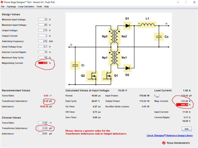
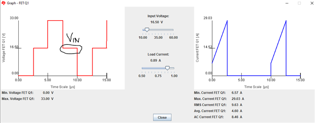
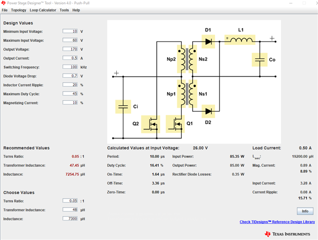
We have designed push pull converter using IC UCC3808-2.  Input is 10 ~ 60V DC input from battery and output is 170V DC.  Generated 170V DC is fed to inverter to get 110V AC output.

Please check attached snapshot of design.


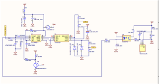
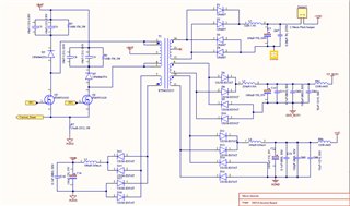
transformer primary inductance is 0.308uH (3 turns on each winding) and secondary inductance is 1.53mH (63 turns).  Board is up successfully and tested with load of 60W.

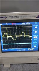
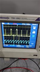
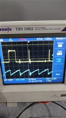
Issue with the board is, Vds waveforms of Q5 and Q6 is not as per ideal waveform.  Ringing observed on Q5 when Q6 is turned on and vice versa.  Also there is ringing in current sens waveform.  Please check images of waveforms for your reference.

 Ch 1: current sense input to IC U5; Ch 2: Q6 Vds

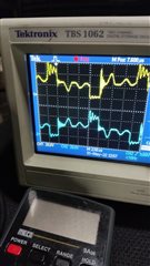
 Ch 1: Q5 Vds; Ch 2: Q6 Vds

Can you help me to resolve this errors in waveforms?  Let me know if you need any other information.

Thanks and regards,

Ankit

  • Ankit,

    The high frequency ringing is due to resonance between your transformer leakage inductance and MOSFET Coss. This is normally controlled by adding dissipative RC snubbers across drain-source of each MOSFET. You should also measure the leakage of your transformer and make sure best practices are used to assure tight primary-secondary coupling.

    If I enter some of your known parameters in TI Power Stage Designer and I brute force to match the inductance values you are using in your design, I get the results shown below:

    You can see that your magnetizing inductance (0.31μH) is too small and needs to be at least one order of magnitude larger (~3μH). A low magnetizing inductance value makes for fewer primary turns but the huge primary current also creates a large di/dt. Here are some comments about your design:

    1. Use TI Power Stage Designer to assure voltages and currents are reasonable - make necessary adjustments as needed
    2. Try removing the RCD clamps on the primary and use simple RC snubbers across each drain-source. When the transformer design is optimized, this should be sufficient to tame the ringing expected on VDS.
    3. Your gate driver (U6) has no VCC cap shown in the schematic? C51 is only good for HF bypass. 100nF is not sufficient for supplying 2Apk current to the MOSFETs. Add something like 1uF-5uF in parallel with C51. What does VCC look like when switching? Zoom in on the edges of the gate pulse and assure that gate switching is not pulling down on VDD. I expect there is some dip on VCC if only 100nF is currently being used?
    4. UCC3808 (U5) needs a HF bypass cap on VDD. Add 100nF directly at VDD pin to GND.
    5. Feedback compensation doesn't look correct for Type 2 compensator typically used for peak CMC in buck derived topology. the TI Power Stage Designer includes a snubber design tool and compensation toll you can use to check your loop.
    6. Looks like you may not have enough capacitance on VBAT. PP is a buck derived topology that produces pulsed input current and needs a decent amount of Cin located close to the transformer primary center tap. You can see from the plateau in your VDS waveform that it is not flat like below. What does your VBAT look like when switching?

    Thanks for connecting through E2E!

    Regards,

    Steve M

  • Hello Steven,

    As per your suggestion, I increased transformer inductance to 70uH by removing air gap.  Now Vds waveforms and current waveforms are clean and close to ideal waveform. 

    Thank you for your guidance.

    I am facing one more issue.  Efficiency of push pull converter is only 60%.  Details are as below.

    Input voltage: 24V; input current: 3.8A; input power: 91.2W

    Output voltage: 170V; output current: 340mA;  output power: 57.8W

    Efficiency: 63.3%

    Can you help or suggest anything for improving efficiency?

    Thanks and regards,

    Ankit

  • Ankit,

    Loss of efficiency could be dominated by AC related loss such as switching loss (gate drive), transformer core loss, AC resistance, leakage inductance, reverse recovery, etc, or it could be dominated by DC related loss such as conduction loss through MOSFET channel, transformer DC resistance, etc. Check some of your fundamental waveforms and measure which are the hottest components in the design. Transformer, MOSFETs and output rectifiers are the usual suspects.

    Regards,

    Steve M

  • Hello Steven,

    I am working in same direction. I found some inconsistency in waveform.  RC pin is set for 100kHz where as Vds signal shows 40kHz frequency. 

    Waveform at RC pinWaveform at primary Mosfet Vds

    Can you check and suggest anything? 

    Apart from this, you suggested to use power stage designer for loop calculator but I am not able to derive values from that and push pull topology is not supported in that.  Can you share any document or reference design for pushpull configuration loop calculator?

    -Ankit

  • Ankit,

    The push pull is a double ended forward topology so the oscillator is running at twice the transformer frequency. If you want your transformer operating at 100kHz, then your oscillator needs to be setup for 200kHz. You may need to tune the exact RC values for the oscillator since what you are currently seeing is not exactly 2:1.

    Here is what your design looks like in TI Power Stage Designer. Check your transformer ratio, LMAG and LOUT values:

    Also, TI Power Stage Designer will work for compensating your loop. The push-pull is a CMC forward and your compensation is a type 2 isolated (w/ inner loop). Make sure your comp configuration represents what is shown below:

    Attached are some design resources for the push-pull topology that I hope will help.

    Push Pull.pdf

    slyt790b.pdf

    slyt813.pdf

    snva553.pdf

    Steve

  • Hello Steven,

    My switching frequency is 100kHz and Vds waveform frequency is only 25kHz.  Please check waveform again and share your views again,

    For loop compensation,  I tried with the tool again and got below results.

    On tool, we are getting fco at1.28kHz and not getting any recommendations for compensation values.  Can you suggest where we are doing mistakes during loop compensation calculations?

    Thanks and regards,

    Ankit

  • Ankit,

    The PWM output should be 1/2 the oscillator frequency but you are reporting it is 1/4 - this does not make sense? Can you please show a scope plot of the oscillator operating at 100kHz and both gate drives operating at 25 kHz? Please be sure to make the gate drive measurements directly at the PWM output and not at the MOSFET VGS? Please use full voltage and time scale with markers to clearly show the measure frequency?

    Regards,

    Steve M

  • Hello Steven,

    Please check below images as you requested.

    As you can see, pulse width is not constant and thats why, Vds waveform is distorted.  Can you suggest any solution for this?  schematic PDF is also attached herewith for your reference.


    200VA_Inverter_Rev1B.pdf

    Primary inductance is 34.4uH; secondary inductance: 15.6uH and primary leakage inductance is 0.24uH.

    Reagards,

    Ankit

  • Ankit,

    Regarding the frequency error you mentioned, I'm not seeing it from the latest scope plots you shared? The plots you shared show the oscillator operating at F=100kHz and the OUT operating at F/2=50kHz and this is normal and operation. There are many other things possibly wrong with the converter but the controller and programming the oscillator seems to be working as expected.

    I recommend you strip this converter down to the very basic things needed to begin a systematic debug. For example, temporarily disconnect all other outputs (VP BOT1, +VC, VBIAS) and only focus on the one that's being regulated (+VDC), disconnect the VDD bootstrap bias winding and temporarily use a DC lab supply to bias the PWM, short the secondary to the primary and temporarily bypass the isolated opto feedback, remove the RCD clamps on each of the main MOSFETs, make sure the capacitance between VBAT and PGND is spilt and located as close as possible to Q5, Q6...similar to the input capacitance requirements of a buck converter, a pp converter has pulsed input current.

    When you have the converter stripped down to the very basic essentials, next make sure the power stage values are acceptable according to what you see from TI Power Stage Designer. Transformer mag inductance, secondary inductance, peak currents manageable for given freq, input voltage, load, etc.

    Once the power stage values are known to be valid, stabilize the loop without the opto at first. Here's an approach that's always worked for me:

    1. Stabilize the voltage loop by temporarily placing a dominant pole in the feedback of the voltage error amp. A 100nF cap between COMP and FB should accomplish this. The regulation and transient response will not be good at this point but that's ok - the voltage loop will be guaranteed stable.
    2. Next, stabilize the current loop. Make sure the CS resistor is the correct value for the given load range you are planning and the Lmag you've chosen for the transformer. Check the CS signal over the full line/load range, add about 20% design margin above worst case corners, adjust your RC filter value corner frequency to minimize ringing but still introduce a linear ramp to the CS input. What is the purpose of R51 - why are you dividing down the CS signal in place of using the correct value for R7. If power dissipation in R7 is a problem then consider a CS xfmr?
    3. Once the CS signal is stable, go back and bias the opto/TL431. The entire feedback circuit does not look correct to me? What is the purpose of D35, D36 and how does any current flow through the opto LED? Make sure your opto is biased and responding over the full line/load range. If this is not correct, the FB will not be correct and this is what determines your duty cycle (along with the CS signal). TL431+opto is a very popular feedback technique for switching converters and you can find many good design resources and YouTube videos on how to properly set it up.
    4. Once the opto/TL431 are properly biased and transferring the error signal to FB correctly and operating over the full dynamic range, remove the short between secondary and primary and connect the opto/TL341 back into the feedback. The converter should now be stable but will still need compensation of the voltage loop.
    5. To compensate the voltage loop, use the TI Power Stage Designer or Excel or MathCad or your simulation tool of choice to model the loop. Otherwise, if you have access to a network analyzer, you can measure the open loop gain/phase and build the compensation in the lab to shape the control loop response until you achieve your desired gain, crossover and phase response.
    6. Once the CS loop, voltage loop, opto/TL431 are all stable, begin to systematically add back the circuit blocks that were previously disconnected

    One last suggestion, if you are not doing this already, please make sure you are measuring all signal "tip and barrel", which means using a short GND spring on your scope probe and measuring directly across the component of interest. This is especially important when looking at control signals and CS signals. Your measurements show lots of noise and I question if it's real or an artifact of noise being picked up from the flying "pigtail" GND lead of your scope probe?

    Regards,

    Steve M

  • Ankit,

    I notice you rejected the answer I provided above? Did the suggestions made not help to debug your converter power stage and stabilize your control loop? If the suggestions I made did not help, please provide details, measurements and waveforms showing which were unsuccessful? 

    Regards,

    Steve

  • Hi Steven, 

    Due to some mistake we clicked on rejected button so you can ignore that and thanks for giving quick response.

    One more thing is we got that DC-DC converter design from Webench and we attached that pdf file which was generated when we inserted our requirement parameters so you can also check that one more time.

    I will follow your guidelines and test our design and let you know result very soon. If you find any other things please let us know.

    Thank you. 

      WBSchematicUCC3808D-2.pdf