This thread has been locked.

If you have a related question, please click the "Ask a related question" button in the top right corner. The newly created question will be automatically linked to this question.

dc dc converter 12v to 48v. High power.

Other Parts Discussed in Thread: LM51561, UC3843, LM5122

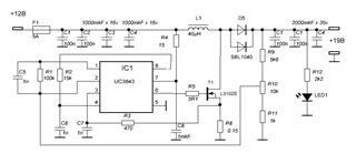
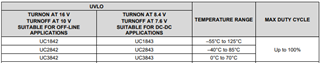
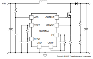
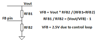
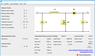
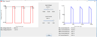
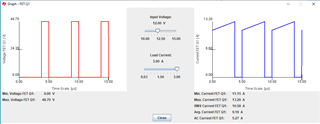
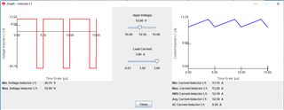
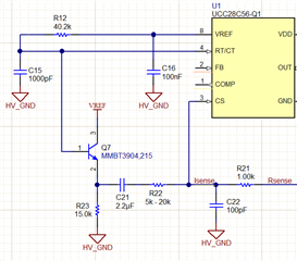
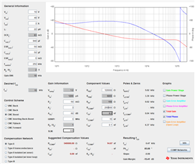
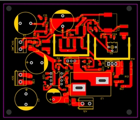
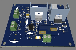
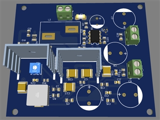
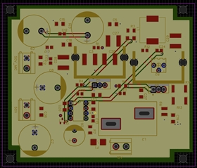
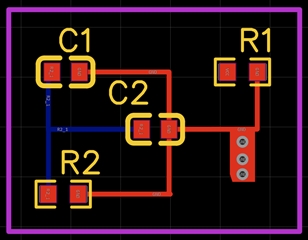
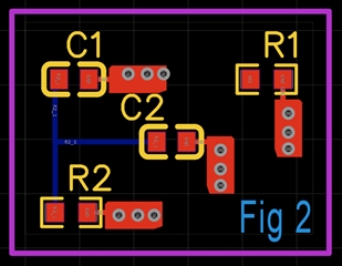
I need a 12-14V to 45-50V battery converter.

The converter should be adjusting min 45V to max 50V. Power not less than 100 watts. Low voltage ripple. Please advise the chip and circuit for this.

I want to feed a very high quality low frequency amplifier from this unit.

Thank you!

  • Hello Gennadiy,

    I would need more information to refine the recommendation.  Not less than 100 W is vague.  Exactly what ripple voltage do you need?  What operating temperature range do you need - consumer, industrial, or automotive?

    The output ripple of any switcher can always be reduced with a second-stage LC type filter.

    Based on the limited information you provided today I would take a look at the UCCx808A-x, and the UCCx808x push-pull families.

    Regards,

    Eric

  • I have a Hi-Fi low frequency transistor amplifier circuit. Its RMS = 65W, supply voltage 50V. But the peak power can be much higher. I can't know exactly what the peak power will be. Therefore, I would like to have an additional power reserve.

     The main power supply of the device is carried out from a 12-14V battery.

    Operating temperature range consumer/automotive. Class AB amplifier generates a lot of heat. This must be taken into account when taking into account the temperature regime. I would also like to avoid using a transformer. If possible.

    I do not know much English. If I couldn't explain something, please ask again.

    Thank you!

  • OK.  Avoiding a transformer is an important requirement.  I think a BOOST topology makes more sense for your application.

    I used TI's online WEBENCH designer with the following requirements;

    VIN = 8V to 18V (more realistic for automotive), Vout = 48V, Iout = 2A (96W).

    WEBENCH produced a design based on the LM51561-Q1 controller.  The PDF report is attached below.

    48Vo, 2A Boost.pdf

    The report has quite a bit of detailed information:  Schematic, BOM, operating conditions, efficiency, etc.

    I hope this provides a good starting point.

    Regards,

    Eric

  • I apologize in advance for my poor knowledge of English.

    Unfortunately, there is no LM51561 chip on sale right now.

    There is a UC3843 chip. Chokes of various inductances are also available in the store. I found several circuits, but I am not satisfied with their parameters. I don't understand what the output voltage depends on. I also did not find a working frequency for UC3843. What can be the maximum?

    My battery is like a car battery. I would like that the DC-DC converter could work with an input voltage in the range of 10-15V. The output voltage was regulated in the range of 45-55V. Maximum current up to 3A. Please help me choose a circuit. Or tell me other chips that can be used. And I will check their availability in stores.

  • Hi Gennadiy,

    The UC3843 or UC3843A can work for you.  They have Vin UVLO Start/Stop thresholds of 8.4V/7.6V.

    The output voltage depends on the feedback resistor divider from Vout to the FB pin:

    The first page of most data sheets show the maximum switching frequency:

    TI has a nice power design tool, POWER STAGE DESIGNER This tool analyzes the power component requirements and can be used with many different topologies.  You should watch the training video.  Choose BOOST and enter your Vin, Vout, and Iout specifications.

    Regards,

    Eric

  • Thank you!

    I would like to know if the UC2843AN chip will fit? I didn't find any difference in the datasheet other than usage temperature.

    Is it possible to use the maximum frequency. Like 450MHz? Or is it better to use 250MHz for more stable operation?

    I didn't find the multiplication factor formula for FB input and resistive divider. Tell her please.

    I apologize for my bad english.

  • Should I use a regular diode or a schottky diode?

  • Hi Gennadiy,

    The UC2843AN is the same controller, just higher temperature rating.

    Usually, customers use a medium frequency, like 200 kHz (not MHz).

    For any regulator, the ratio of the feedback resistors (RFB1 and RFB2) depends on Vout and VFB:

    Regards,

    Eric

  • Hi Gennadiy,

    For the boost diode a schottky would be the best because it will have the lowest forward voltage drop and dissipate the least amount of heat.

    However, the boost diode must be rated for at least Vout_max (55V in your case).  It may be difficult to find a schottky rated this high.

    Regards,

    Eric

  • Hi again,

    I used Power Stage Designer to calculate the RMS current in the boost diode, the FET, and the inductor with your typical operating conditions.

    The following data will help you choose components.

    DIODE:

    MOSFET:

    INDUCTOR:

    You should download and use Power Stage Designer.

    Regards,

    Eric

  • Good afternoon. Thank you!

    I tried to match the details to the circuit. Unfortunately, I don't know how to find the part values, which I circled in red.

    And, I'm very nervous that I chose the wrong parameters for the details that are already on the diagram. I had never assembled power devices before and had never dealt with inductors. Since this circuit has huge ripple, I want to put in a filter. What current should the inductance L2 be rated for?

    Here is the inductance L1 - www.mouser.bg/.../VER2923-223KL

    Here is the transistor - lcsc.com/.../MOSFETs_Infineon-Technologies-IRF3710PBF_C2562.html

    Here is the diode - https://lcsc.com/product-detail/Super-Barrier-Rectifier-SBR_Diodes-Incorporated-SBR20100CT_C507838.html    It seems that this diode fits the parameters. But they are in the body 2. What should I do with my free leg? Do not connect anywhere?

    Capacitor -  lcsc.com/.../Aluminum-Electrolytic-Capacitors-Leaded_Nichicon-UPW2A471MHD_C433298.html

    Resistors 0.125W.

    Do any parts of the device need to be placed on heatsinks?

  • The secondary inductor (L2) can be rated about 3A.  No need for 15A in that position.

    Connect both diodes in parallel.

    Your input voltage is relatively low.  For the R/C values to VCC I would start with 1 or 2 ohms and 1uF to 2.2uF.

    Calculating compensation components (FB to COMP) is one of the challenges of a boost regulator.  Here is one application note from TI that might help:  https://www.ti.com/lit/an/slva636/slva636.pdf?ts=1654802983383&ref_url=https%253A%252F%252Fwww.google.com%252F

    There are many other articles on the web about boost compensation.

    I'm sure the diode needs to be on a heatsink.  The MOSFET probably should have a heatsink too.

    Regards,

    Eric

  • So, if you could (eventually) find some LM5122 controllers you could replicate this reference design from TI.  The following link shows test results, schematics, BOM, layout files, gerbers, etc.

    https://www.ti.com/tool/PMP21274

    This is a synchronous boost (no diode).  It significantly reduces losses and achieves much higher efficiency.

    Eric

  • Good day. Unfortunately, it is not possible to buy the LM5122 chip now. A few things won't help. This device we expect to sell 20-30 pieces per month. Therefore, we need those parts that are consistently in stock.

  • Please check my schematic. Have I selected all the components correctly?

    What power should the resistor R5 be used? 5 watts or 10 watts?

    Is it necessary to repeat the output filter on L2 and C7-C11 to reduce ripple? Or just add 4 more capacitors to the existing filter? This is a power supply for a high end low frequency amplifier and I need minimal ripple.

  • The 470uF capacitors I use for the filter have the characteristics

    ESR 76mΩ@100kHz and Ripple Current 1.31A@100kHz

  • I order my PCBs from China. Therefore, if I make a mistake, I will have to wait a month to correct the problem. I'm very concerned.

    I apologize for bad english.

  • Hello Gennadiy,

    R5 will conduct the same current as the MOSFET.  So the power can be calculated with ~(13Arms)**2 x 0.1ohms x MaxDutyCycle.  I think 3W should be adequate.  If you want to be conservative, have the option for two 3W resistors in parallel, but only populate one.

    It is good to have options for a secondary output filter to reduce high frequency noise, especially for your application.  You may not need the filter but best to include it in the PCB layout.  I think 4x 470uF + 1x 470uF is more than enough.  Maybe place 2x 470uF on each side of L1 (4 total).

    The specifications for the 470uF electrolytic capacitors look relatively good.  However, to address very high frequency noise (MHz region) it is best to include some ceramic capacitors too.  You should have some ceramic capacitance in parallel with both C5 (input) and C9 (output) and C7/C8 (output #2).  It's important to have the ceramic capacitor(s) located as close as possible to the controller.  See PCB layout recommendations below.

    Is 0.1 ohm for R5 low enough?  The current limit will occur at 1V/0.1ohms = 10A, which is too low.  The peak currents can be at least 13A or more.  The value for R5 should be reduced to less than 75 mohms.  Maybe start with ~50 mohms.

    You need to include an RC low pass filter between R5 and the Isense pin to remove current (switching) spikes.  I would start with 1k and 100pF.

    Also, for peak current mode control with duty cycles above 50%, you must have a "slope compensation" circuit.  Without slope compensation current mode control is unstable above 50% duty cycle.  We typically use an NPN transistor as an emitter follower to buffer the RT/CT voltage and AC couple it into the Isense pin.  Here is what slope compensation and current sense filtering should look like:

    Lastly, the error amplifier compensation circuit is not entirely correct.  R13 should be changed to a capacitor (about 100pF) to form a high frequency roll-off of the gain.

    One final note.  PCB layout is an important part of constructing any switch mode regulator.  The following application note discusses the important aspects of layout for a boost regulator.  Pay attention to minimizing the loops around the input and output capacitors.

    https://www.ti.com/lit/an/slva773/slva773.pdf?ts=1654869304360&ref_url=https%253A%252F%252Fwww.google.com%252F

    Regards,

    Eric

  • Hello again Gennadiy,

    I entered your specifications into Power Stage Designer and used the Loop Calculator to obtain better compensation values.

    Note that I used a 50mohm sense resistor (Rs), and 2x 470uF electrolytic (940uF) along with 5x 10uF ceramic (50uF) output capacitance.

    Based on this analysis you should start with R6=250k (presently 6.81k), C3=15nF (presently 1nF), and R13=100pF (presently showing 100k).

    At 10Vin and 3A load your crossover frequency will be 0.47 kHz with a phase margin of 85 degrees.  The gain margin will be 15.4 dB.  This is a very stable operating point.

    Regards,

    Eric

  • Eric, thanks a lot!

    I tried to fix all the errors. But I'm not sure that I connected the transistor correctly.

    And a question about R12. Is it possible to replace 250K with 249K? Or is it better to add another 1K resistor in series? 250K is hard to buy now.

    What is the approximate ripple for this circuit? Maybe you need to add a 15 µH inductance and a regular 4700 µF capacitor?

     Thanks again!

  • Hi Gennadiy,

    It's OK to use 249k for R12.

    I think you can remove C10 and C11.  C7 and C8 (2x 470uF) should be adequate.

    Also, C5 is quite large (470uF).  To save some cost and PCB area I think 22uF or 47uF would be more than enough.

    The output voltage ripple after the second filter should be very low;  10's of mV.

    Regards,

    Eric

  • Eric, I'm afraid I misunderstand English.

    So excuse me. I want to ask again. The output voltage ripple 10mV is possible if I remove both L3 and C5? Did I get it right?

    Is it better to place the power supply and the low-frequency amplifier as close as possible (ideally on the same PCB), or is it better to place them at different ends of the device?

    I also need to power a condenser microphone (48V). Do I need to make another such unit for this, or can I power the microphone and low-frequency amplifier from one power supply? The condenser microphone preamp board is located approximately 30 cm from the power supply.

    And thanks a lot for your help, Eric!

  • You should remove L3 and C5.

    The PWM switcher will create some noise.  Physically separating it from other sensitive components is a good idea.  Make sure you have adequate bypass capacitors at each downstream device (amplifier and microphone).

    If you are not sensitive to cost, then having two power supply units seems to make sense.  Maybe you can have provisions for two independent power supply units but start by populating only one.

    Two more things.  Whenever a switcher has noise issues we do two things.  1.  Add a resistor between the OUPUT pin and the gate of the MOSFET (include provisions for 1206 size resistor, but start with 0 ohms), and 2) Add an R/C snubber from the SW node to ground.  The following paper discusses boost noise.  See section 2.4 for placement and calculations for the RC snubber.

    https://www.ti.com/lit/an/slva790a/slva790a.pdf?ts=1655142562228&ref_url=https%253A%252F%252Fwww.google.com%252F

    Eric

  • Eric, thank you for your advice.

    R / C snubber from the SW node, I did not add to the scheme. I have read that it is impossible to calculate. It is necessary to measure the necessary data on the working power supply. Perhaps I misunderstood?

    I have now assembled the board. Could you take a look. Perhaps I made mistakes?

    The printed circuit board is four-layer. Here are its characteristics.

    Size: 95.5mm x 81.03mm

    Signal layers: 4

    Components:50

    Venues:106

    Surface pads:71

    Plated through holes: 35

    Through non-plated holes: 0

    Holes:8

    vias:20

    Chains:17/19

    Track length:1120.35mm

    Copper areas: 2

  • Even if the snubber were impossible to calculate, you should include options for RC snubber, in case you need them.

    I see one via in many places.  If you're connecting to ground or Vin there should be 3 or 4 vias at each connection point.

    Make sure the Vin and Vout loops are small, like the layout guideline shows.

    Regards,

    Eric

  • Eric, thanks!

    I already thought the same thing, that it was necessary to leave free places for the RC chain.

    I wanted to ask. Perhaps there are some universal R and C values that can be set? Let this RC chain be not ideal, but better than none.

  • Maybe I just can't understand you because of translation difficulties. This is my first time trying to make a four layer board. Please take a look, is that what you mean?

  • It is better to part the earth with paths on the top layer. Or all the elements that are connected to the ground to be connected with vias?

  • I made Vin as short as possible and placed it on the top side of the board. Vout made the copper area the second layer.

    Vout Looks like this. This is right?

  • Yes, multiple vias looks good.

  • Thank you!

    And what about the RC values. Is it possible to install some standard ones? Or is it necessary to leave empty spaces?

  • You can start with 220 pF (100V) and 220 ohms.  Make sure the resistor is a 1206 size, or larger because it will dissipate a low/medium amount of power.

    Eric

  • Thank you so much!

    Last question.

    It is better to spread the earth with paths to the top layer? Or should all elements that are connected to ground be connected via vias?

  • Using the ground plane is easiest layout.  If you place the ceramic input and output capacitors to minimize the loops it should be good.

    Eric

  • I'm afraid that I may misunderstand English. Therefore, if it is not difficult for you, please clarify again. How right. Like in the first picture or like in the second picture?

  • Hello Gennadiy,

    For a ceramic capacitor (which filter high frequency), it is best to have vias located at the capacitor.  Locating the vias at the capacitor minimizes the trace inductance and allows the ceramic capacitor to have optimal performance at high frequencies.

    As for grounding, I found a very good reference on PCB routing of a boost regulator.  In the following article, pay attention to how they minimize the input and output power loops when placing the power components, and use a dedicated signal ground for the control components.  A dedicated signal ground prevents the power ground from coupling into the control.  This is good standard procedure for any switching regulator.

    https://www.powerelectronicsnews.com/the-dc-dc-boost-converter-part-3-power-supply-design-tutorial-section-5-3/

    Regards,

    Eric

  • Eric, thanks for the link! I thought about it a lot. But I don't understand how to minimize this area. Heat sinks interfere. Perhaps you can put a diode and a transistor on one heat sink? This would solve the problem.

    Maybe you should immediately put the resistor R6 some minimum value? Now R6=0

  • When you do the place and route do your best to make the loop small.  Don't place the diode or MOSFET far from each other.  If possible, connect the source of the MOSFET to the low side of Cout on 1 layer, then make the connection to ground.  Don't use vias in that loop.

    You can start with R6=0 and increase the value when the PCBs arrive.

    This thread is 2 weeks old and hasn't closed.  Please consider clicking RESOLVED and open a new thread if you need further assistance.

    Thanks,

    Eric

  • Eric, good. I'll try again and close the topic. Is it possible to put a diode and a transistor on the same heatsink or is it a bad idea?

  • It's not a bad idea if the heatsink can dissipate all the heat and keep the diode and FET cool.  The diode is usually one of hotter components so I'd prefer to see it on it's own heatsink.

    Eric

  • Good. I understand.

    Thanks again!