Hi
sorry bother you guys again.
the output volt ripple is 850mV at 1.5A Io
and i found SW note is unstable
please see my attachment.
the conditions as below
Cin:22uF*3+10uF
Co:22uF*2
Vin: 4.2V
Vo: 3.3V
Io: 1.5A
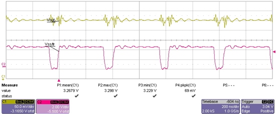
Hi
sorry bother you guys again.
the output volt ripple is 850mV at 1.5A Io
and i found SW note is unstable
please see my attachment.
the conditions as below
Cin:22uF*3+10uF
Co:22uF*2
Vin: 4.2V
Vo: 3.3V
Io: 1.5A