This thread has been locked.

If you have a related question, please click the "Ask a related question" button in the top right corner. The newly created question will be automatically linked to this question.

TPS7B81-Q1: TPS7B8150QDGNRQ1

Part Number: TPS7B81-Q1

Hello,

I have Doubts regarding MPN-TPS7B8150QDGNRQ1.

Our Requirement is : Input:(6-36V), Output- 5V, 20mA Ambient Temperature-(-40 - 105degC)

1) Since I am using this circuit for wake-up supply so I connected EN Pin directly to input. So I want to ask what is the maximum current in the enable pin so that this pin will not damage.

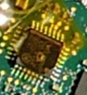
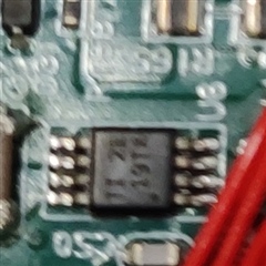
2) I check this IC for Overload Condition at 25degC , so through electronic load I increase the current & at 210mA the output of the IC drops & when I observe the temperature of this IC for 10 minutes it is around 100.6degC. This temperature is at the top of IC. So can you please help me that how can I find out the junction temperature of this IC at overload condition. Input voltage at this condition is 24V.

See the below graph for overload condition.

3) I also check this IC for thermal shutdown condition at 105degC ambient. Again I increase the current & at 102mA the output of IC drops & when I observe the temperature of the IC for 10 minutes it is around 127.6degC. This temperature is at the top of IC. So can you please help me that how can I find out the junction temperature of this IC at thermal shutdown condition. Input voltage at this condition is 24V.

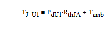
I tried Finding the junction temperature at thermal shutdown condition by below formula

If I consider the junction to case thermal resistance -50.2degC/W as per datasheet, According to my calculation the power dissipation is 2.842W and top temperature is 127.6 degC then the junction temperature at thermal shutdown condition is 270.28degC & In the datasheet it is mentioned that the thermal shutdown temperature is 175degC.

I calculated the power dissipation in case of thermal shutdown as Pd = (Vin-Vout)*Iout = (24-0.314)* 0.102 = 2.842W

Can you please where I am wrong in this calculation. Please find the below graph at thermal shutdown condition.

4) If you observe the overload condition reaches at 210mA & Thermal shutdown condition is at 102mA  so  why this much current difference in both the case. Can you please give me the solid reason regarding this.

If this is related to the thermal resistance so can you please provide me that value.

I hope to get a helpful revert.

Regards,

Ajay Sahu.


  • In Continuation of the same MPN - TPS7B8150QDGNRQ1.

    I measure the top temperature of the IC at 105degC ambient then it is almost 113.6degC. I want to know how can i find out the junction temperature of the IC.

    In the calculation if I use the below formula. then with 0.6W power dissipation, junction to ambient thermal resistance Rtja = 63.9(as per datasheet), ambient temperature is 105degC then the junction temperature comes out to be 143.34degC.

    But in my case since i know the top temperature is 113.6degC, 0.6W power dissipation, and  = 1.8 (as per datasheet)  then the junction temperature comes out to be 114.68degC.

    So calculated value of junction temperature is 143.34degC & measured value is 114.68degC . My question is why this much difference? Can you please tell where I am wrong in the calculation. 

    See the below image where I measured the temperature with thermocouple.

    Regards,

    Ajay

  • Hi Ajay,

    1) I'm not sure what you mean by how much current the enable pin can take into it without causing damage because you have no control over how much current goes into the enable pin. A high enough voltage (> VIN) on EN will damage the enable pin and will likely cause an increase in current that is sunk into the enable pin, but the current is not what is causing the damage in the first place.

    2) The graph you provided shows thermal shutdown and not current overload. This is apparent because with an overload condition the load current would not go to 0A unless thermal shutdown was also triggered. Are you saying that once the VOUT drops when IOUT = 210mA, you then wait for 10 minutes with this condition present and then measure the junction temperature? If that is true, measuring the junction temperature with this condition (cycling in and out of thermal shutdown) is not going to be accurate because you will be measuring the average temperature of the case and not the peak temperature (which is what will cause the thermal shutdown). A better way to measure the junction temperature is to find the load current that causes thermal shutdown, and then reduce the load current by a small amount until the device stops going into thermal shutdown and then measure the case temperature. This will result in a peak junction temperature measurement. 

    3) You should use the equation Tj = P_D * ψJT + T_top. The reason for this is that the thermal resistance parameters (the Rθ parameters) are application dependent, specifically board layout dependent, but the ψ parameters are much less application dependent and provide a more accurate calculation in a real application. Using your calculation of Pd = (Vin-Vout)*Iout = (24-0.314)* 0.102 = 2.842W is not useful because this is the power dissipated once the device has already entered thermal shutdown and so the VOUT has fallen and hence increased the power being dissipated in the device. Under this condition the device will repeatedly enter thermal shutdown and will never reach the junction temperature that you would calculate using this power. Please try the recommended procedure in note 2). 

    4) The difference is because of the difference in ambient temperature. When the ambient temperature is higher the device can dissipate less power before reaching thermal shutdown.

    For your follow-up question:

    Your calculation using ψJT is the correct approach here. I do not understand the picture you provided because it does not show any package that TPS7B81-Q1 is available in. Can you confirm that you are calculating the junction temperature of the TPS7B81-Q1 and not another IC?

    Regards,

    Nick

  • Hello Nick,

    Thanks for the reply,

    In continuation with your reply further some doubts are there,

    1) Point 1 is clear regarding Enable pin.

    2) Point 2 is also clear that "A better way to measure the junction temperature is to find the load current that causes thermal shutdown, and then reduce the load current by a small amount until the device stops going into thermal shutdown and then measure the case temperature. This will result in a peak junction temperature measurement. ". So Nick I am measuring the Top temperature of the device in this case so do you mean that after measuring the Top temperature I should use the formula Tj = P_D * ψJT + T_top for measuring junction temperature. where power dissipation in this case is Pd = (Vin-Vout at condition where device stops going into thermal shutdown i.e. 5V in my case)*Iout at condition where device stops going into thermal shutdown i.e. 150mA in my case. ?

    3) Point 3 related to point 2 so it will also clear once you reply point 2

    4) Point 4 is also clear

    Regarding my follow-up question..Yes I am measuring the top temperature of TPS7B81-Q1 I only show you a dummy image for your understanding. As I am measuring the top temperature & after measuring the top temperature I should use the formula Tj = P_D * ψJT + T_top for junction temperature as you said.

    So Nick my doubt is in our documentation analysis (THEORITICAL CALCULATION ANALYSIS) we generally use Tjunction = P_D * RthJA + T_AMBIENT for finding out the junction temperature & after finding out junction temperature we use T_case = T_Junction - P_D * RthJC for finding out case temperature.

    But in testing after measuring the top temperature I am using Tj = P_D * ψJT + T_top for calculating junction temperature

    So In case of Tjunction = P_D * RthJA + T_AMBIENT I am getting JUNCTION TEMPERATURE as 144degC & In case of Tj = P_D * ψJT + T_top I am getting JUNCTION TEMPERATURE as only 114degC.

    So can you please tell how I can co-relate these two results as both are junction temperature & this much difference is this valid? Can you please give a solid explanation regarding this as we are facing same problem in all TI IC's

    Would you suggest that we need to use Tj = P_D * ψJT + T_top in our documentation as we are using two different formula & getting two different results?

    Can I consider Tj = P_D * RthJC  + T_case where T_case = T_top for verifying results?

    Please find below the actual image of TI where at the top i am measuring temperature.

    I hope to get a helpful revert.

    Regards,

    Ajay Sahu


  • Hi Ajay,

    2) Yes your understanding is correct on all points. 

    So Nick my doubt is in our documentation analysis (THEORITICAL CALCULATION ANALYSIS) we generally use Tjunction = P_D * RthJA + T_AMBIENT for finding out the junction temperature & after finding out junction temperature we use T_case = T_Junction - P_D * RthJC for finding out case temperature.

    This is not correct. The equation Tjunction = P_D * RthJA + T_AMBIENT is only used during the design process because the ambient temperature is usually the only known temperature in the system during the design phase. In a real application, RthJA is very dependent on the board layout, so its usefulness is lost once the board has been assembled and powered. The equation you mentioned, T_case = T_Junction - P_D * RthJC, is never used like this. To use this equation, it would be in the form T_Junction = T_case + P_D * RthJC, where you measure the T_case and plug in the P_D and RthJC as before. With that said, the equation Tj = P_D * ψJT + T_top is more useful anyways because the ψ parameters are much more accurate in a real application. 

    So can you please tell how I can co-relate these two results as both are junction temperature & this much difference is this valid?

    These are different because RthJA is not constant and is very dependent on board layout. Also as I mentioned above, measuring the junction temperature while the device is cycling in and out of thermal shutdown is not going to produce a result that seems to make sense because the junction temperature you would measure is the average junction temperature during its warming and cooling cycle and is not a steady-state measurement. So to reiterate, do not rely on the RthJA equation in a real application; instead use the ψ parameters. This will be a much more accurate junction temperature estimate. 

    Can I consider Tj = P_D * RthJC  + T_case where T_case = T_top for verifying results?

    In a real application you should avoid using the thermal resistance parameters (θ) and instead you should use the ψ parameters. The reason for this is in the way the parameters are defined. The θ parameters assume that all of the heat is leaving through the respective area of the package. E.g. the RthJT assumes that all of the heat leaves the package through the top. These metrics allow the customer to understand how heat leaves the package through its various areas on the package. Of course in a real application, heat does not only leave the package through only a single side of the package, which is where the ψ parameters come in. The ψ parameters are defined assuming that the heat leaves through all outlets as it does in a real application, which makes them much more useful in a real application, and they remove almost all of the dependency of the board layout.

    So in summary, if you measure the top of case temperature during steady-state when the device is not operating in a thermal shutdown cycle and use the equation Tj = P_D * ψJT + T_top this will be the most accurate measurement.

    Regards,

    Nick