This thread has been locked.

If you have a related question, please click the "Ask a related question" button in the top right corner. The newly created question will be automatically linked to this question.

BQ76952: Question about BQ76952

Part Number: BQ76952
Other Parts Discussed in Thread: TIDA-010208

Hello:

I have a question about bq76952:

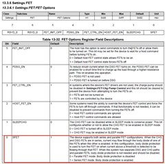
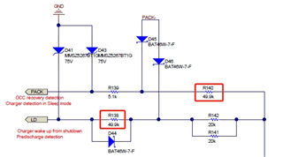
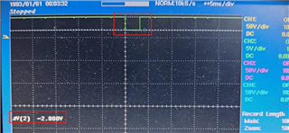
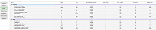
When we use it, the configuration has enabled the SFET bit, that is, the MOS is used in series. Theoretically, when charging, the bq76952 should turn on the discharge MOS, no matter whether there is discharge protection or whether the external MCU controls to turn off the discharge MOS, because it has the "body diode protection" function. The threshold value of the body diode is 50mA. When charging, I can see that CC2 has 101. The user current unit is 10mA, so the threshold value of 50mA should have been met. However, the MOS transistor was not opened and did not play the role of body diode protection. So the question is: where have I not set it yet, right? Or what should we pay attention to?

  • Hey Jimmy,

    One common issue I see regarding body diode protection is that people are using the DFETOFF pin to turn off DSG FET. This will not allow body diode protection to activate. How are you disabling/enabling the discharge FET?

    Thanks,
    Caleb

  • Hi Caleb:

    Thank you for your reply. We do use the DFET_OFF pin to turn off the discharge FET (the same is true for charging, because we use the low side application scenario). Can we be sure that if we use this function, we need to control the FET manually? That is, when MCU detects discharge, it should turn on the charging FET, otherwise, it should turn on the discharging FET? This is OK for us, but there is a problem to be confirmed. When AFE is internally protected, can the discharge FET be forcibly turned on through DFET_OFF pin?

    We have another problem here. We use the following recommended circuit (51K for R140) at the PACK pin, but the pack voltage and LD voltage we have obtained are not accurate. We have measured the related state of the PACK voltage:

    Our problem is that the obtained pack voltage is not accurate. The actual battery PACK voltage is 42.337v, while the measured value is 38.6v. We did the following tests:

    1. use a multimeter to measure the voltage on the PACK pin, and the display is consistent with the PACK voltage;

    2. when the oscilloscope is used to measure the PACK  voltage, the following conditions are found: when the chip collects the PACK  voltage, the PACK  voltage will actually be pulled down by about 2.8V;

    3. if there is a 2.8V voltage drop on the 51K resistance, the current absorbed during measurement is about 55ua, that is, the presence of R140 will indeed interfere with the sampling of pack voltage.

    So: we want to reduce the resistance of R140, R139, R138 and R142 to reduce the acquisition error as much as possible. We plan to change it to about 5.1k. But the question is, will there be any problem if we reduce it?

  • Hey Jimmy, 

    Since you are using the DFETOFF/CFETOFF pins deactivate the FETS, you will not be able to turn them back on by any means until you release the FETOFF pins. It also disables body diode protection. Even if you try to activate the charging FET manually during discharge it will not turn on. I will have to get back to you on.

    If you need to turn off the any of the FETs immediately, you could activate the D/CFETOFF pin and then immediately send a DSG_PDSG_OFF/CHG_PCHG_OFF command, and then release the C/DFETOFF pin. This would allow body diode protection to work.

    The circuit you shared was used in a TI Reference Design (TIDA-010208) that had the requirement of handling a regenerative braking voltage of up to 120V, which is why the resistor values are so high.

    You can reduce the resistor values to fit your design requirement. Normally we recommend 10k resistors on the PACK and LD pin.

    Thanks,
    Caleb

  • Hello Caleb:

    Thank you for your reply!
    1. What if I protect the body diode by my software, which means turn on the dsg fet by dsg_off_fet pin, after the software detect charging current? Does it possible to protect the body diode under dsg protection condition ( like under voltage protect condition ) also?
    2. So if we still want the BMS servive under 120V regenerative braking voltage, we'd better to keep using 51k right? Do you have a way to calculate how big the resister we need to use under different regenerative braking voltage?
    3. It's OK for my software to compensate the pack and ld voltage, Because from our testing, the leakage current of the sample circuit inside bq769x2, it's about 55uA. Which means it's easy to get the real voltage by Vs + Vc, Vs is the voltage read from bq769x2, and Vc is calculated by 55uA * Rin.

  • Hi Jimmy,

    I think using the software to compensate the Pack and LD voltage is necessary when using the larger resistors since the device expects 10k normally. What voltage do you expect for this application? 

    Body diode protection is active in all cases when one of the FETs is disabled except when DFETOFF or CFETOFF is held low. So if a protection is triggered or if FET commands are used, it will still be active.

    Best regards,

    Matt

  • hello Matt &  Caleb:

    I got another question about entering the sleep mode.
    1.Sleep setting:

    2.We discharge battery to CUV protection, and check log data.

     So the question is: 

    1. Does bq769x2 have another way to enter sleep mode, except the conditions below? It looks like the bq769x2 enter sleep mode immediately after CUV protection present.
    2. Or maybe some where we set uncorrect?
    3. And it looks like the "sleep hysetersis time" not correct also, I tested the time by my watch, if I set to 30s, it's about 15s the chip sleep, and if set to 60s, it's about 30s.

        Please check the attached file for all my setting, just if you want to!

    M001_ALI.gg.csv

  • Hey Jimmy,

    Your sleep settings look fine.

    1. The device is allowed to go into sleep mode after receiving a fault. The four seconds between fault detection and seeing the device in sleep mode could have been enough time below the sleep current threshold to allow the device to sleep.

    2. Just to clarify, sleep hysteresis is the minimum time required to pass before the device is allowed back into sleep mode after waking up. It is not a required time for the device to stay in sleep mode.

    Thanks,
    Caleb

  • hello Matt &  Caleb:

    Thank you for your reply, and they are really helpful.

    Normally we need 120V for the P+ port, so I think the 49.9k should be fine for our application. But just want to know how to calculate them, and maybe we need to modify them in some application.

    And for another question:

    In our application with other AFE, we sometimes need to reset the OCD errors by MCU ( like recover from OCD protections by some special customer operation ), so the question is does BQ769X2 have a command which can force it recover from OCD protection? Or maybe I'd better to set the AFE recover automaticlly after OCD protection with very short time, and MCU take the error mask, and turn off mosfets, and do the recover stuff?

  • Hey Jimmy,

    Yes you can recover the AFE from OCD using the MCU. You would just need to clear the alarm/alert registers. I would say it's up to what the system requirements are. You can recover from OCD relatively quickly by controlling the AFE with the MCU. You can have the device generate a signal on the ALERT pin instead of turning off the FETs, and then let the MCU handle everything.

    Thanks,
    Caleb