This thread has been locked.

If you have a related question, please click the "Ask a related question" button in the top right corner. The newly created question will be automatically linked to this question.

TPS793: LDO latches up (?) or otherwise conducts a ton of current

Part Number: TPS793
Other Parts Discussed in Thread: TLV320ADC3101, TPS7A20

I'm designing a battery-operated device, and I use the TPS79330DBVR to supply the AVDD for an ADC chip (TLV320ADC3101).

The ADC can be configured to consume close to nothing and this is used when the device is sleeping, to conserve battery.
However, the TPS79330, being a low-noise/high PSRR design, consumes 170µA when on, hence I need to use its EN pin to turn it off when the device sleeps. To this end, I've designed the following circuit around it:

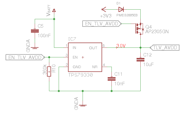
The idea being that,

  • when the device sleeps, EN_TLV_AVDD is 0V, the TPS79330 is turned off (<1µA), and TLV_AVDD is supplied through the 3.3V rail, D1, and Q4. Thus the TLV320 will still receive AVDD, but it would be noisier
  • when the device is active and needs to record audio, EN_TLV_AVDD is 3.3V, the TPS79330 is on (~170µA), and Q4 is off, preventing 3.3V/D1 from interfering

VBatt ranges from 3.3 to 4.2V.

This circuit assumes that the TPS79330 wouldn't mind if the output is at non-zero voltage with EN=0.

I have four prototypes assembled with this schematic, and all exhibit this strange behaviour:

  • If I supply the VBatt rail from a bench PSU (which I assume ramps up the voltage smoothly) all is well - the LDO works as expected, and the powersaving scheme works too (e.g. with Vbatt=3.6V, and EN=3.3V, I get TLV_AVDD=2.99V; with EN=0V, TLV_AVDD is 3.06V and is noisier)
  • If I use the actual battery (connection point is though a pin header), the LDO heats up a lot and does not work:
    • device temperature is upwards of 120°C (measured with a thermal camera). If VBatt is high enough it exceeds beyond 180°C and one of the prototypes had the TPS79330 release its magic smoke
    • the NR pin drifts around around 200mV
    • the EN pin consumes a ton of current, as it is 0V if commanded 0V, but gets only to ~2.3V when commanded with 3.3V, I believe because of the MCU pin's limited drive capability
    • Vout is basically Vin when EN=3.3V, and around 0 otherwise

I suspect a latchup, caused by the combination EN = 0V and noisy/uncoordinated rise on Vin and Vout (since the 3.3V rail comes from another LDO, fed by VBatt).

There's some slight variability as one of the device exhibits the problem on battery regularly, but not always. The other two have this problem every time. All devices work fine with the PSU supply.

Any idea of what's causing the latchup (if it is a latchup)? And how to resolve it?

I can poke around anyone has an idea what to try/measure.

  • Hey Vesselin,

    If it is possible, could you provide a scopeshot of Vbat/PSU, TLV_AVDD, EN_TLV_AVDD and Iout of the system at startup?

    Also would it be easier to adapt a different device like TPS7A20 that could be left on as to replace the extra architecture?

    I hope this helps!

    Thanks,

    -Jimmy

  • OK, thanks, will try to provide a scopeshot, probably on Monday.
    I understand that the TPS793xx series are old and probably not the best performance for the Iq compared to the modern alternatives. We'll look into these as well, but likely not the TPS7A20, as it's not stocked anywhere we normally shop from.

  • Hey Vesselin,

    Sounds good.

    Maybe we can try to suggest some other lower Iq alternatives with 3V Vout in SOT-23 package that might have better availability.

    Thanks,

    -Jimmy

  • Hello Jimmy,

    I was able to poke around a bit, sadly I am not able to measure Iout of the system as it is simply not practical to rip up a trace and insert a shunt there. There is some pattern to the failure modes, which might be able to shed light into what's happening.

    Please look into the pictures here.

    In all scopeshots, the yellow trace is Vbat/PSU (2V/div, nominal ~3.6V in both cases), the pink trace is EN_TLV_AVDD (2V/div, nominal 0/3.3V), and the blue trace is TLV_AVDD (1V/div, nominal 3.0V)

    • Shots 00 and 01 show startup (00=PSU, 01=Battery), at 2ms and 5ms/div respectively, sorry for the mismatch. Apparently the system 3.3V LDO waits some 13ms to start. The circuitry supplying EN_TLV_AVDD does some minor blip when energized, but otherwise EN stays low; the nonzero TLV_AVDD in both cases comes from that system 3.3V rail, through D1 and Q4.
    • Shots 03 and 04 show the same thing (03=PSU, 04=Battery) at 50ms/div. As you can see, the PSU one is clean; the Battery one has a glitch at ~80ms where the TPS79330 suddenly starts to consume tons of current (because the Vbatt suddenly got a tad lower. Battery/protection internal resistance is around 0.15 ohms). While taking that trace, the TPS got mightly hot
    • Shots 07, 08 and 09 show a different failure mode that's even more bizzare. Apparently, what happens is:
      • At 13ms, the system LDO starts. This somehow causes Vbatt to sag very deeply (?)
      • At 22.5ms, EN becomes HIGH, and Vout momentarily blips up, but is then off again. Keep in mind that at 22.5ms, the EN pin is not actively driven - why it becomes high is a mistery
      • At ~80ms, again, the high current drain condition (Vbatt→TLV_AVDD) appears. Vbatt drops a bit due to source impedance. TLV_AVDD raises to ~0.2V. Shot 09 shows that glitch zoomed in.

    All this is very puzzling. Let me know if I can measure anything else that can shed light?

    Kind regards,
    Veselin

  •  Hey Vesselin,

    We are still trying to find out what is happening here and we have a couple more questions.

    What is driving the EN_TLV signal? How is it changing from 3.3V to 0V

    Is there any other load besides the ADC and what is the expected load current?

    Is it possible to measure the input current to the LDO with a current probe? Also if possible, the EN pin current?

    Thanks,

    -Jimmy

  • Hi Jimmy,

    answering your questions:

    • EN_TLV is driven from a CMOS output - one of the pins of an I/O expander, the MCP23008
    • No other load besides the ADC. Load current <1µA at idle and 3-4mA when conversion is on per datasheet. I'm not sure what the current is when the TLV320ADC3101 powers on. I'd believe it's something intermediate as the ADC itself is not actively operating, but OTOH is not configured in the lowest power state. Likely ~1mA
    • Will try to do. The EN and Input signals are on longer traces that can be ripped up

    BTW, I completely forgot to mention that I do have another prototype, exactly the same PCB and schematic, that has TPS70933QDBVRQ1 instead of TPS79330DBVR. That LDO is not really suitable for the application for its higher noise figure, and also it's 3.3V out. The technician populated it by mistake. However, it does not exhibit the latch up issue described in this thread.

  • Hey Vesselin,

    I see the EN_TLV signal spikes to 2V in the scope shots when the output goes to 3V. This is interesting and should have an impact on the system.

    Was there any point when the output voltage of the LDO (TLV_AVDD) was greater than Vbat? Maybe the ADC was powered on while Vbat was low or disconnected. 

    Scope shot 07 shows a moment where the output voltage is greater than Vbat. 

    Thanks,

    -Jimmy

  • Hi Jimmy,

    many thanks for your continued attention to this thread! We really appreciate it!

    Yes, I saw that EN_TLV spike as well and I found it a bit odd as well. As you can see in the schematic, there's a 360k pulldown on the EN pin, to ensure proper 0V during powerup conditions. My guess is that when the MCP23008 is initially powered on as the 3.3V rail ramps up, it momentarily glitches. I can verify whether this is true it by measuring other (uncommited) MCP23008 I/O pins.

    As per the "TLV_AVDD > Vbat" suspicion, yes, it may be possible for a brief time, about a millisecond. The TLV_AVDD, when supplied through D1 and Q4, ultimately comes from the battery, through another 3.3V CMOS LDO (AP2112K-3.3V if that's important). So in theory, that voltage, especially after D1, should be always lower than Vbat. However, some loads are on the Vbat rail, not on the 3.3V. The biggest is one Vbat→5V boost converter, which we enable at some point in the startup sequence. When it initially surges to fill the output cap of the 5V rail, the Vbat may sag momentarily. The Vbat rail does not have a lot of capacitance on it, whereas the 3.3V rail has something to the tune of 50-60µF. So it's possible that the 3.3V rail stays relatively stable while Vbat dips below it for a brief moment. One hint in that direction is that we tried unsoldering D1 on one of the prototypes and with that, the TPS79330 did not exhibit the issue.

    However, removing D1&Q4 is only practical if the TLV320 would not mind having AVDD unpowered (~0V) while DVDD is always on (1.8V) and IOVDD is always on as well (3.3V). I guess this warrants a second question to TI, if we choose to fix the latchup issue by removing D1&Q4.

    As per the EN/Input current measurements, I'm trying to fit these into the schedule and do them today or tomorrow at the latest.

    Again, thank you for your persistence!

    Regards,
    Veselin

  • Hey Vesselin,

    No problem. Hopefully the current measurements might shed some more light on what is happening here if the device was not damaged by reverse current. Were you able to repeat these results using new units?

    As for the question about the TLV320, you could start a new thread with just that question or we could find an applications engineer for that product and ask internally.

    Thanks,

    -Jimmy

  • Hi Jimmy,

    here's what I found:

    1. I first cut the trace between the MCP23008 and the EN pin of the TPS79330 and replaced it with a 100Ω resistor. Plugging in the scope probes as before reveals the issue is still present. The current through the 100Ω is practically zero - so I guess the issue is not (always) caused by the EN pin consuming any serious current
    2. Then I cut the trace from Vbat feeding C5/TPS79330 input. I replaced it with a 10Ω resistor (I tried with 56Ω first, then repeated with 10Ω). In both cases the issue is gone; the TPS79330 is working as expected. I coded a test program that toggles the EN signal each 5 seconds. When the TPS79330 is enabled (and Q4 is open), I see clean 2.999V on TLV_AVDD. When the TPS79330 is disabled, and Q4 is closed, I see noisy 3.062V on TLV_AVDD. Likely the LDO itself has not sustained any damage.

    So it really seems the very rapid power-up when I connect the battery voltage mechanically (or the contact noise/bounce) is the culprit?

    I'll ask a separate question about the TLV320's behaviour with AVDD=0. If that one works, it would be a cleaner solution than hacking in some 10Ω which are far from proven to fix the issue reliably.

  • Hey Veselin, 

    Jimmy is out of office today, we will need to look into this and get to you on Monday. 

    Thanks, 

    McKyla

  • Hi all,

    just letting you know that we tried placing another LDO in place of the TPS79330; it is the MCP1802T (again a 3.0Vout LDO in SOT23-5, with somewhat lower Iq). It is in the same circuit, in one of the prototype devices, and it does not exhibit the issue.

    Maybe the best course of action for us would be to ditch the efforts of trying to make the TPS79330 work, and instead just replace it with the MCP1802T.

  • Hey Veselin, 

    My apologies for the delayed response and this issue that you are having with the TPS79330. It seems like this a reverse current issue. If you wanted to further help troubleshoot with the TPS79330 there are a couple things that you could try. One thing that would be using a Schottky diode from OUT to IN to prevent this reverse current issue. 

    Thanks, 

    McKyla

  • Many thanks, McKyla!

    I was able to test that suggestion, with a 1N5817 schottky diode, and indeed this resolves the issue, and it seems like a reliable fix. Charging a battery now, so that I can test with Vin=4.2 as well.

    The only worry with the suggested fix is that we need to be careful with diode's reverse current. Many jellybeans like the 1N5817 may be many µA or even mA reverse current at elevated temperatures (our max design temperature is 60°C), and that would cause the AVDD voltage to increase above 3.0V due to reverse conduction through the diode. But I believe we'll figure this out.

    Again, thank you all for your effort. I'll verify some more and will mark the question as resolved after that.

  • Hey Veselin, 

    You're very welcome, I am glad that this resolved the issue. I am going to close this thread, if you have an additional questions or follow up please feel free to reopen it. 

    Thank you, 

    McKyla