This thread has been locked.

If you have a related question, please click the "Ask a related question" button in the top right corner. The newly created question will be automatically linked to this question.

UCC28634: fault cause codes

Part Number: UCC28634

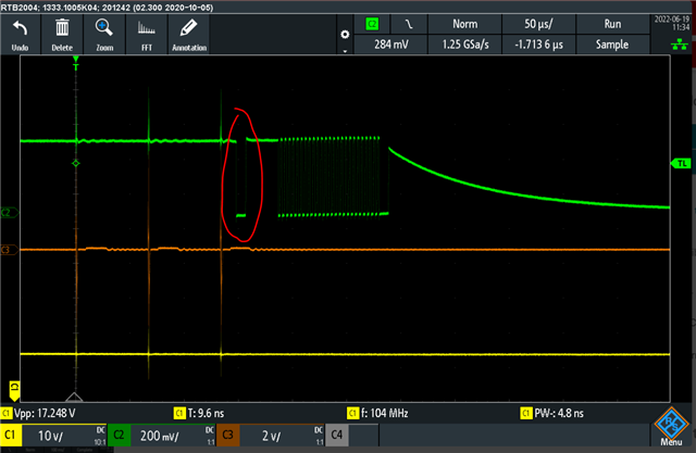
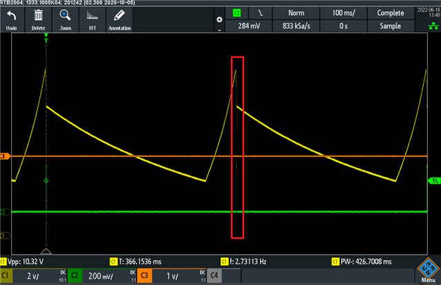
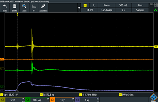
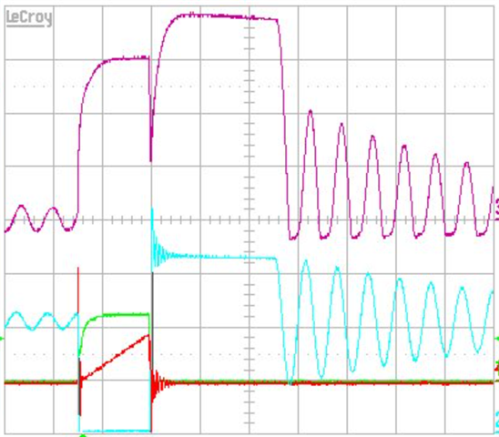
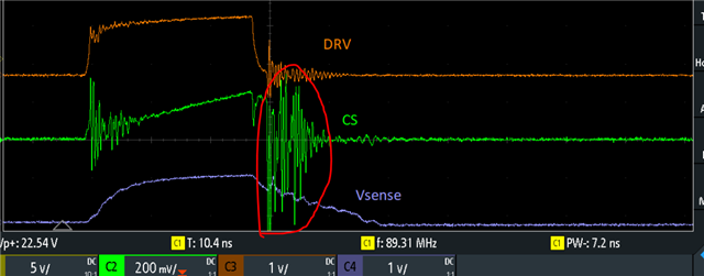
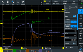
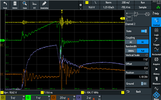
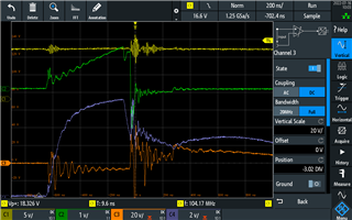
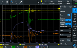
I'm troubleshooting a power supply design based off the UCC28634, and I've tracked it down to a fault code on the SD pin giving 25 - AC (i.e. bulk cap level) under-voltage detection before startup or restart

Codes taken from this thread - e2e.ti.com/.../ucc2863x-fault-cause-codes

I'm running it off a DC power supply set to 130v

I'm now looking for the next step to sort out this fault code.
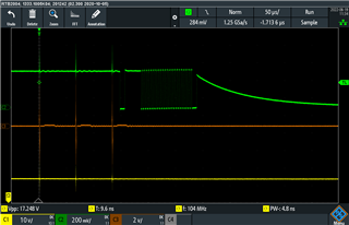
Green - SD pin

Yellow - Vdd pin

Orange - AUX Winding

  • Hi, Daniel:

    Would you please share the test condition and schematic for further discussion?

    It seems something happens in your SD pin. As you can see as below, the SD drops in a red circle, and the thread you shared is similar to yours. 

    I would suggest you to check your SD related circuit to check if it operates correctly. 

    Regards, 

    Wesley

  • Hi Wesley

    Attached is the Regulator Schematics as generated from Webench 

    I have nothing currently connected to SD

    RegulatorDesign.pdf

    Thanks,

    Dan.

  • Hi, Daniel:

    Please add a resistor like 470kohm to SD pin first to see if it helps. 

    It has possible to make SD pin influenced by noise if we let it floating. 

    Thanks

    Regards, 

    Wesley

  • Added 470kohm pulldown to SD pin, no change

  • Hi, Daniel:

    Thanks. Now it seems to be clarified this fault is not from SD fault. 

    Would you please zoom in this area as below to check if the fault from OVP triggered?

    You may also refer the application note as below link to check if any faults mistriggered during start-up process. 

    https://www.ti.com/lit/an/slua783/slua783.pdf?ts=1655777618099&ref_url=https%253A%252F%252Fwww.google.com%252F

    Regards, 

    Wesley 

  • This is the peak at the area you've highlighted

  • Hi Daniel,

    My apologies for the delay in response. Wesley is currently out of office. We will respond to you next week.

    Regards

    Manikanta P

  • Hi Daniel,

    Thank you for the query.

    From your plot above is the purple curve the voltage on VSENSE pin? Its seems there VSENSE during demag time is not correct.

    For an initial debug, can you please run with the an Vin less than startup voltage level of 113Vpk/80Vrms) and capture VDD/ CS/DRV/AUX/VSENSE to observe the reset behaviour of VDD with 3 drive pulses as shown below (unloaded case with just preload resistor).

    Then increase Vin above the startup level, VSENSE should be something like the right figure.

    I would also recommend to decrease the startup resistor on the HV pin to 180k to get a faster startup.

    As a second step, for debug purpose , please try connecting an external dc source to VDD through a blocking diode. Set this external Vbias to say 10 V or so, high enough to stay above the UV level but not high enough to get over the start threshold. current limit it to, maybe 10-20 mA max.

    Now connect the external Vbias first, with the high voltage input turned off. Then apply the high voltage input, HV will charge VDD from the starting external Vbias level to the start threshold, then the IC switching and bias power will pull VDD down, but it should get caught by the external Vbias and keep the IC running and check on the error due to bulk capacitor voltage level.

    Kindly share the above waveforms to help debug.

    Thank you

    Regards,

    Harish

  • Hi Harish,

    Here are the waveforms that I get.

    They do not significantly change with low or high voltage level input

    The external Vbias DC source of 10V caused no output at all from the IC


    Thanks,

    Dan.

  • Hi Daniel,

    Thank you for the reply. From the last which you attached aux winding waveform should be negative when the DRV pulse is high. Can you please check the polarity of your aux/bias winding once. Also do you have a 5 ohm resistor after the rectifying diode D3 used for generating VDD? Can you please share the full schematic?

    Thank you

    Regards,

    Harish

  • Hi Harish,

    I have swapped the polarity of the aux winding to be correct now (I had swapped it a few times previously, in case I had it wrong), no significant changes in the other waveform traces though.

    This 5 ohm resistor, would that be in series with D3 before the Vdd pin? I will give that an attempt. Edit: No change with resistor added.

    The schematic is have is exactly as generated out of Webench

    2100.RegulatorDesign.pdf

    Thanks,

    Dan.

  • Hi Daniel,

    Thanks for the reply and confirming on the polarity of the auxiliary winding.

    There are a couple of concerns from the plots attached:

    1. The first plot which you attached has oscillations on the VDD pin is over 20V which potentially exceeds the max. capability of this pin which makes me suspect the leakage. Can you let me know the leakage inductance of your transformer?

    2. DRV signal signal is only 1V. Can you check the three exploratory pulses when VDD reaches max value?

    Thank you

    Regards,

    Harish

  • Hi Harish,

    DRV had a 10:1 probe that wasn't configured in the scope to show that, so I don't think there is an issue with the DRV signal.

    I am measuring the leakage inductance as ~13uH.

    I'm not 100% sure I am measuring it correctly, but I have shorted all the transformer windings except for the primary input and then I'm measuring the inductance of the primary with an LCR meter.


    Thanks,

    Dan.

  • Hi Daniel,

    Thank you for the reply. Considering your magnetizing inductance from the calculator 526uH, 13uH leakage is less than 3% of Lpri, hence should be fine. Did you try adding the resistor which I told to aux winding Vdd cupply. Also try increasing the Cvdd to 22uF. Please let me know your observations after making these changes.

    Thank you

    Regards,

    Harish

  • Hi Daniel, 

    Was there any developments in the test results with the above suggestions?

    Thank you

    Regards,

    Harish

  • Hi Harish,

    Sorry for the delay. 

    I did the AUX Vdd resistor, no change.

    Cvdd has been a total of (measured) 23uF all throughout as well, with a 10uF ceramic and a 10uF electrolytic and a 0.01uf ceramic right on the chip.

    One of my questions that hasn't been answered is what are the conditions that make this error occur -> 25 - AC (i.e. bulk cap level) under-voltage detection before startup or restart


    Thanks,

    Dan.

  • Hi Daniel,

    Thank you for the reply.

    Further examination of your waveforms indicate CS exceeding the abosolute max value of -0.3V when the switch is turned off as shown below.

    There are a couple of things which you can try to reduce the ringing on the aux.winding:

    1. Try replacing the schottky diode on the auxiliary winding with an ultrafast diode like ES1D-13-F with a fast recovery time of less than 25ns. There is definitely current flowing through the parasitic capacitances (of the MOSFET) which also has to be addressed. 

    2. On your question regarding error 25 (AC UV level), this should be present as an UV detected through the Vsense pin during ON time (which is a function of turns ratio and upper resistor Rs1). Can you please capture the above waveform (VSENSE/AUX) displaying the voltage and time scales as these are not visible in the above image?

    Please let me know your observations once you have run the test with the above changes.

    Thank you

    Regards,

    Harish

  • Hi,

    I have the fast diodes on order, and I'll update when I get them.

    Thanks,

    Dan.

  • I have swapped in an ultrafast diode ES1D-13-F, no change.

    I have captured these waveforms with all the scales showing

    Thanks,

    Dan.

  • Hi Daniel,

    Thank you for sending the waveforms.

    I was trying to take a step back to verify your schematic which you had shared. Seeing your current parameters of Lpri-526uH and Rcs of 470mohm seems to obey the design constraints for Np=57, Ns=7, Na=8 turns. The parameters obtained sem to be consistent with the AC input voltage and the inductance is optimized for minimum bulk voltage/V_boundary of 62V as shown in the screenshot below:

    In the above case, the volt sec for output sampling design constraint seems 

    But the value of primary inductance seems to be very less when calculated as above. When I use the design calculator and design for Vreflected=120V and V_boundary=100V (which is your minimum input voltage of 100Vdc to 160Vdc), the minimum inductance comes close to 900uH and the sense resistor will also be different as shown below:

    Can you please confirm/recheck your design calculations and cross check it with excel calculator? Please let me know if you require any clarifications.

    Regards,

    Harish