This thread has been locked.

If you have a related question, please click the "Ask a related question" button in the top right corner. The newly created question will be automatically linked to this question.

UCC28950: Transformer voltage got distorted and Power supply going out of control.

Part Number: UCC28950
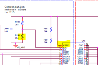
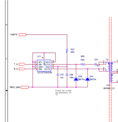
Other Parts Discussed in Thread: UCC28951

Hi Mike,

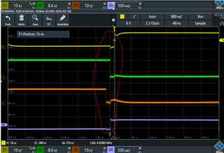
We are doing test our PSFB but have seen some wired behaviours when we reach to the Vin 470V and output of 140V. It is designed for output of 140V@20A. Do you have any suggestion from the waveform attached?

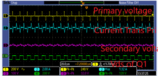
YELLOW: Voltage across primary winding

Blue: Primary Current

Purple: Voltage across secondary winding

Green: Vds of Q1 (Leg-1 top SiC)

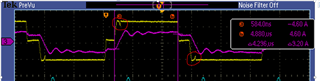
It seems to me that we are going out of control and peak current suddenly went up to 18A which is not obvious. However Q1 voltage looks ok and also bottom half of transformer voltage looks ok.

Top half side of the transformer voltage is completely destroyed. Also it is exactly the point where I think closed loop start regulating? 

NB: Ignore the current direction on both the waveform it was just that current clamp meter was connected in different direction hence two current appearing out of phase. Just to avoid confusion.

Would appreciate your quick support on this.

Working at low line voltage.TIFNot working case.TIF

  • Hello,

    It sounds like you might be saturating your transformer or the design is going into hiccup mode over current protection.  Section 7.3.14 of the data sheet explains hiccup mode over current protection in detail. https://www.ti.com/lit/ds/symlink/ucc28950.pdf

    If you evaluate Comp, CS, SS and Vout you should be able to figure out what is going on.  Please note when evaluating comp you should add a 1 k ohm between Comp and the scope probe.  

    The following link will bring you to an application note on how to design the FSFB with the UCC28950.  You may find this helpful.  It also has a link to an excel design tool that you can use to check your design. https://www.ti.com/lit/an/slua560d/slua560d.pdf

    Regards,

  • Hi Mike,

    Thanks a lot for your comments. There was problem with Rsense value might be but we changed it to 20R now. But what surprising is that after changing the Rsense to 20R now we are experiencing a different issue. at very low voltage itself the voltage is becoming very narrow pulse between primary of the transformer(pls see the attached image1 and 2) and going to on and off mode.

    Even with higher voltage of 400V its same behaviour...What could be the issue if you could suggest pls?? 

    We have used 72K for DELAYAB and CD, same which is as per xls it is around 800ns. Seems like it is entering in burst mode and remains, load is already connected though..

    I am wondering if it is going in burst mode continuous or hiccup mode. Iprimary does not looks high to go to hiccup mode, load is also connected so not sure why burst mode remains with even >400V, Tmin is currently 12.4k. Any recommendation would be great.

    Many Thanks,

    Amit

    .....8780.TEK00004.TIF

  • Hello,

    Could you label your waveforms to what the channels are and what your load conditions are?

    You have an image 4 and 2, was one of them supposed to be 4?

    When it comes to the narrow pulses is your output voltage being maintained?

    Regards,

  • Hi Mike,

    Please see the waveform with label. Image_1

    It stays in burst mode. I have increased voltage from 0 to 400V, but always stays same. Output does not keep constant as pulses comes and goes. Please refer image 2. load is connected three 36 ohms 1kW resistors in parallel ( resultant resistor is 12 ohms ,3kW) connected.

    Initially I thought it might be because of very low input voltage but  then observe that burst waveforms stays for whole voltage range.

    Appreciate your support.

  • Hello,

    I think you are design may be going into over current protection(OCP).  Section 7.3.14 describes the over current protection mode in detail.

    https://www.ti.com/lit/ds/symlink/ucc28950.pdf

    The below information describes how this function works.

    To see if your design is going into hiccup mode.  You will need to evaluate Comp, CS, SS and Vout.  If it is going into OCP protection the SS capacitor will be charging and discharging per figure 42 above.   Please note when evaluating comp you should add a 1 k ohm between Comp and the scope probe.

    If it is going into this mode it could be a couple of things.

    1. Noise on the CS pin going above 2V, can solve with a 1k ohm 220 pF low pass filter.

    2. Transformer is saturating due to too much slope compensation or too much filtering at the CS pin.

    The following link will bring you to an application note on how to design with the UCC28950 in FSFB.  It reviews setting up slope compensation to avoid having the design operate in voltage mode control.  You can also use it to review your design.

    https://www.ti.com/lit/an/slua560d/slua560d.pdf

    Regards,

  • Hi Mike

    Thanks for your reply. We did further test and found that PS enters in hiccup mode as you have mentioned.

    By increasing sense resistors we could go upto higher voltage but again it entering in hiccup mode when it reaches to the desired output voltage and closed loop compensation start working.

    In this case output was set to 48V and hiccup starts when it reaches to 48V

    CH1: CS signal

    CH2: Comp signal(which seems disturbed)

    CH3: Primary voltage

    CH4: secondary voltage

    What could be issue of going in hiccup mode when compensation starts? We are not saturating transformer...

    3438.TEK00011.TIF1638.TEK00012.TIF

    times with different value of Rs it goes to hiccup even before reaching to final output value. In this case output was set to 140 V and hiccup starts earlier .

    CH1: CS signal

    CH2: Comp signal(which seems disturbed)

    CH3: Primary voltage

    CH4: SS Signal

    3757.TEK00016.TIF

    While lower voltage ramping up and working conditions do you see any issue with SS signals CH4?

    TEK00017.TIF

  • Hello,

    Reviewing the latest day and will get back to you shortly.

    Regards,

  • Hello,

    You should be decreasing the current sense resistor so it enters OCP later instead of earlier.  Increasing the CS resistor will make it go into OCP earlier.

    Also when doing this monitor the current and bring up the design slowly, to make sure nothing is over heating or any magnetics are getting saturated.

    I look at your CS waveforms not sure why you put the scope on AC for this?   It should be DC referenced.

    There is low frequency ringing on the CS signal that should not be there.  Please make sure the CS transformer is front of the H Bridge and not in series with the primary of the transformer.  If it is in series with the transformer you can lose the DC information and low frequency ringing similar to what you observing is present.

    One last thing this design looks like it had a maximum duty cycle above 90%.  If you need duty cycle greater than 90% you should use the UCC28951 instead of the UCC28950.  The following link will bring you to an application not that explains why the UCC28951 is a better choice for designs with greater than 90% Duty Cycle.  https://www.ti.com/lit/pdf/slua853

    Regards,

  • Image_1.TIFImage_2.TIF4024.TEK00005.TIF6180.TEK00008.TIF8512.TEK00007.TIF5050.TEK00006.TIF

    Hi Mike,

    Many thanks for taking time and thanks for your support so far.

    Q1: Regarding CS Pin, I am sorry for typo, I was actually meaning bringing down the CS pin slowly down to avoid OC trigger and going into burst mode. I think now we have the right CS Rsense setting where we do not see anymore OCP triggering issues like before.

    And it was in DC mode, but I guess while measuring different signals I forgot to change the mode in scope setting from AC to DC.

    In summery, I think Rsese issue is now well understood and tuned properly for the converter operation.

    Q2: Position of CS: Its is in front of the H bridge not in series. Regarding LF ripple I am explaining our situation below and could be the reason, you can comments better here.

    Q3: What I have seen the problem is now appearing when closed loop starts kicking, I mean when it reaches to the desired output voltage converter is going out of control .

    For ex, the test we have performed on last week, we are getting output of 136V at ~445Vinput, (pls refer Image_1 CH1: Primary voltage CH2: Current CH3: secondary voltage) and everything looks fine till that point but as soon as output reaches 140V at ~455V input, converter's waveform is getting disturbed (pls refer Image_2 CH1: Primary voltage CH2: Current CH3: secondary voltage).  If you see image_2, primary, current , secondary voltages (CH1,2 and 3) the duty cycles are not consistent at all, Though output 140V is still stabilized from 455V to 470V but a wired audible sounds from transformer we can hear. I don't understand this Disappointed ( Is this because of situation I have explained in Q4...!!!!)

    Also when it happens, COMP signals is really disturbed, all the signals like CS, SS, COMP is having lot of noises. connecting scope probe was causing more noise from the transformer but after removing the probe a little reduced but it is still disturbed and noises are audible. We have also connected a LP filter of around 488kHz frequency but just a very little improvement.

    Q4.We have a very small output capacitor of only 4uF ( yes , it is only 4uF) and big inductor L of 1H (yes, it is 1H with 12 ohm R) , what I am suspecting if this small 4uF capacitor is the culprit here causing all noises, LF ripple on CS, not able to cope up with the duty cycle changes when suddenly duty cycle starts changing dynamically once the output reaches to its set point? What do you think here? I did a PSpice simulation and if I change my C from 2000uF to 4uF, all the measurements like COMP pin, CS, are really noisy as well...What do you think? 

    Q5.Do you think delay setting is a problem here ( pls refer TEK0005-6 CH1: QA CH2:QB CH3:QC CH4:QD)?

    Q6.We do not have SR rectification though we have the controller setting with DCM pin and ADELEF, do you think those settings really matters when we do not have SR mode?

  • Hello,

    Please see my comments below.

    Q1: Regarding CS Pin, I am sorry for typo, I was actually meaning bringing down the CS pin slowly down to avoid OC trigger and going into burst mode. I think now we have the right CS Rsense setting where we do not see anymore OCP triggering issues like before.

    And it was in DC mode, but I guess while measuring different signals I forgot to change the mode in scope setting from AC to DC.

    In summery, I think Rsese issue is now well understood and tuned properly for the converter operation.

    > O.K.

    Q2: Position of CS: Its is in front of the H bridge not in series. Regarding LF ripple I am explaining our situation below and could be the reason, you can comments better here.

    > Is the CS transformer in front of the HBRIDGE?

    >Could you please attach a schematic that I could review?

    Q3: What I have seen the problem is now appearing when closed loop starts kicking, I mean when it reaches to the desired output voltage converter is going out of control .

    For ex, the test we have performed on last week, we are getting output of 136V at ~445Vinput, (pls refer Image_1 CH1: Primary voltage CH2: Current CH3: secondary voltage) and everything looks fine till that point but as soon as output reaches 140V at ~455V input, converter's waveform is getting disturbed

    >This waveform looks like your UCC28950 is operating over 90% duty cycle.  If you need more than 90% duty cycle you need to use the UCC28951.

     https://www.ti.com/lit/pdf/slua853  This could contributing to the instability.

    (pls refer Image_2 CH1: Primary voltage CH2: Current CH3: secondary voltage).  If you see image_2, primary, current , secondary voltages (CH1,2 and 3) the duty cycles are not consistent at all, Though output 140V is still stabilized from 455V to 470V but a wired audible sounds from transformer we can hear.

    >This looks like the converter is going from minimum duty cycle to maximum duty cycle. Maximum duty cycle is great than 90%.  The transformer current does no look correct at max duty cycle.  There may be something incorrect your schematic.

    >When looking at comp it required to add a 1k ohm resistor between.  If you do not due this you will see stability issues.

    I don't understand this  ( Is this because of situation I have explained in Q4...!!!!)so when it happens, COMP signals is really disturbed, all the signals like CS, SS, COMP is having lot of noises. connecting scope probe was causing more noise from the transformer but after removing the probe a little reduced but it is still disturbed and noises are audible. We have also connected a LP filter of around 488kHz frequency but just a very little improvement.

    >

    Q4.We have a very small output capacitor of only 4uF ( yes , it is only 4uF) and big inductor L of 1H (yes, it is 1H with 12 ohm R) , what I am suspecting if this small 4uF capacitor is the culprit here causing all noises, LF ripple on CS, not able to cope up with the duty cycle changes when suddenly duty cycle starts changing dynamically once the output reaches to its set point? What do you think here? I did a PSpice simulation and if I change my C from 2000uF to 4uF, all the measurements like COMP pin, CS, are really noisy as well...What do you think? 

    > 4 uF of output capacitance sounds pretty small for your output capacitor.  The output capacitor does affect your voltage loop compensation.

    >Your output inductor is also quite large.

    >I am just curious what your input and output power requirements are? 

    >Did you use the excel file in application note SLUA560d to double check your design?  It will give guidance on selecting the output inductor and output capacitance for your design.  https://www.ti.com/lit/an/slua560d/slua560d.pdf

    Q5.Do you think delay setting is a problem here ( pls refer TEK0005-6 CH1: QA CH2:QB CH3:QC CH4:QD)?

    >The delay setting should only affect ZVS and should not cause a stability issue.

    Q6.We do not have SR rectification though we have the controller setting with DCM pin and ADELEF, do you think those settings really matters when we do not have SR mode?

    >Not using SRs should not have an effect on the stability.

    Regards,

  • Hi Mike,

    I think schematic is correct. I can't share sch here, would you kindly message me your email ID.

    Regards,

    Amit

  • Hello,

    All technical support on the e2e is handled publicly.  If you cannot share your schematic that is O.K.  Maybe you can try to contact your local Texas Instruments Field Applications Engineer to help further if needed.

    Regards,

  • Hi Mike,

    I have attached it here. R and C values are tweaked during the testing but overall architecture is same, And regarding the duty cycle I have seen the stability issue even with the lower duty cycle case....So I think its may not be only issue of duty cycle here >90%.  Also 1k was connected in series with COMP pin. Pls refer attached sch.

    BTW, do you know who is your local TI support engineer responsible from England?

    Many Thanks,

    Amit

  • Hello,

    Not sure who the field applications engineering team is in England.  I did find this link that should help you get in contact with right TI support teams.

    https://www.ti.com/info/contact-us.html

    The only waveforms I have seen is the converter jumping from minimum to maximum duty cycle.  In the cases were the duty cycle is greater than 90% the UCC28950 is know to have stability issues with OCP protection.  So if your design requires more than 90% duty cycle you do have to switch to the UCC28951.

    At this point I would double check your design with the application note/excel design tool.   This will ensure the design is using the correct input, output capacitance; as well as, your output inductor.  The tool also goes through voltage compensation; as well as, CS slope compensation to ensure the design is  stable.  It is recommended that you also check the voltage loop with a network analyzer and large signal transient testing.

     https://www.ti.com/lit/an/slua560d/slua560d.pdf

    One other thing I could recommend is getting a hold of the UCC28950 600 W evaluation model (EVM).  The following link will bring you to the user's guide for the evaluation module.  If possible you may want to order one of these EVMs to evaluate.  You can compare the waveforms to what you see in the lab and it may help you trouble shoot the design.

    https://www.ti.com/lit/pdf/sluub02

    Regards,

  • Hi Mike,

    Is there a way to slowly bring up the board in open loop? What is the best way control the duty cycle externally, like using a POT (variable resistor) in the feedback path? I would like to control the Pulse width in a controlled way. I think we can connect POT in place of EA- resistor but will it be possible to see PWM variation with change of resistors? Many thanks

  • Hello,

    Set up the voltage as a follower, EA- to EAOUT,  Setup a resistor divider of a separate bias to EA +.  Then you can put a pot in either the high side or low side to control the voltage.  Or you could adjust the EA+ voltage with the bias supply.

    Regards,

  • Hi Mike,

    Thanks for your reply. I have connected a POT in place of R195 instead and I could see the voltage changes down from 2.5V--->2V-->1V etc but unfortunately there is no change in the duty cycle.

    I am monitoring Transformer primary and it appears to me always >90% duty cycle and does not reflect any variation with changes of EA+ voltage. I am testing at low voltage where input is just 50V and load connected. Am I missing anything?

  • Hello,

    Disconnect your feedback loop tie the EAO to EA-.  Put a voltage divider on VEA+ then you should be able to control the duty cycle.  Please note that you will need to have a CS signal to control as well.

    Regards,

  • Thanks Mike, I am able to control the duty cycle now but seems like it is bit sensitive. I though the variation of the voltage is from 0.5V to 2.5V, but seems like the range is between 0.8V to 2V around...

  • Hello,

    Did you account for slope compensation?  You may be able to get more range by adjusting it.

    Regards,

  • Hi Mike,

    Not really, Rsum is still with the old configuration i.e. 121K, so do you mean by reducing Rsum will have better margin? Good to know this...

  • Hello,

    I reviewed the question again.  Your PWM ramp/slope compensation varies from 0.8V to 2.8V and the CS signal has a 2V cycle by cycle current limit.  So if you are in peak current mode control you should be able to only adjust while the comp is above 0.8V.

    The CS signal is summed with the ramp.  This should produce a 800 mV offset + the slope compensation.  You had mentioned that you were not able to adjust the CS signal with a comp of greater than 2V.  Is this correct or were you referring to the CS signal?  The UCC28950 does have a 2V cycle by cycle current limit that will limit the duty cycle.

    Regards,


  • Hi Mike,

    Thanks for your reply.

    I have done a complete study of duty cycle today. Duty cycle is around 5% when Vcomp is around 0.8V and duty cycle reaches to max when Vcomp is around 1.1V. I can control this well externally with a step of around 140mV which is fine for me for now. Less than 0.8V stops pulsating. 

    My Rsum is connected to GND with 121k ie in peak to peak mode. 

    'You had mentioned that you were not able to adjust the CS signal with a comp of greater than 2V.  Is this correct or were you referring to the CS signal?'--Not sure if we are talking same point, I did not measure the CS signal while testing in open loop. I am still in low voltage setup with 50V input. 

    I understand in peak current mode CS will protect from OC when it exceeds 2V even in open loop. So I want to keep it as a protection so that accidently I don't exceed the current limit while testing it in open loop.

    My question was, is there a way to improve this range of 0.8V to 1.1V?  I have understood 800mV offset in peak current mode, by reducing Rsum will I be able to get more margin? I have increased the Vcomp more than 1.1V but what I have observed that with duty cycle was already max when I have reached 1.1V at VComp.

    Many thanks for your support. 

  • Hello,

    If the duty cycle is greater than 90% chances are the slope compensation is not limiting the duty cycle.  If it was decreasing the slope compensation would allow you to achieve more duty cycle. 

    Your comp range is from 0.8V to 1.1V to achieve full duty cycle.  It is possible that your current sense resistor is too small.  By increasing the CS resistor you should able to get more duty cycle.

    Regards, 

  • Thanks a lot Mike. Will try that.

    Another question, Can we start with Vcomp from less than 0.8V at high voltage (640V?), what is the minimum duty cycle limit?

    Idea is to test it in open loop with HV now but for that first I will established the HV keeping Vcomp <0.8V where PWM is not there and then slowly increase Vcomp for low to high duty cycle. So is there any risk doing this, is there any minimum duty cycle limit?

  • Hello,

    If Vcomp < 0.8V your duty cycle will be less than zero.  The minimum duty cycle is programed by Rtmin, check the data sheet for details on how this function works.  The minimum controllable duty cycle is generally down to 2%.  

    Testing your design open loop is O.K.  I recommend using a minimal load less than 10% to begin with and evaluate the CS signal, input of the transformer switch nodes etc...  For safety you might want to use a DC source and limit the output current to protect phase shifted full bridge.

    The following link will bring you to an application note that you may find helpful in the design.  It will show you how to setup the AB, CD and AF, BE delays.  This is generally done at 10% load.  https://www.ti.com/lit/an/slua560d/slua560d.pdf

    Regards,

  • Thanks Mike, seems working ok now, I am getting bit of noise from transformer when duty cycle is very low. Have not tested complete range of Vcomp yet but tested few duty cycle points >10% to 20% duty cycle where I can control the output by changing the Vcomp at 600V. I have to investigate what causing the noise from transformer at very low duty cycle.

  • Hi Mike,

    Hope you are doing well. What I have found that EA+ is not quite constant sometimes and causing  disturbance in PWM in open loop.

    Currently it is biased from UCC28950 internal VREF by a voltage divider (see pic below) and I am adjusting duty cycle by changing the bottom resister which works well but causing disturbance at sometimes. After checking this voltage, found that when IC start switching, this EA+ is disturbed, sometimes goes up and causing disturbance in PWMs,

    Do you think its the issue because of using VREF of ICs? Do we have to use separate biased power supply and disconnect it from internal VREF of UCC28950  IC? 

    EA- is directly connected to COMP (pin 3 and pin 4 of IC) and no feedback loop.

  • Hello,

    I would think that you should be able to use the reference for the EA + resistor divider.  When you first start up the UCC28950 it will go through a soft start.  Where the UCC28950 charges the soft start (SS) capacitor.  When this occurs the COMP will try to track the SS voltage. This may be causing some of your instability.  So when doing open loop testing start with EA + tied to ground.   Wait for the soft start (SS) capacitor to fully charge. Then you can adjust up EA+ slowly to control the duty cycle with your potentiometer.  This will help remove instability issues during open loop testing.

    Regards,

  • Hi Mike,

    Hope you are well.

    I think I have progressed further, and got my required voltage and 90% power level but of course duty cycle requirements is high and I will have to move to UCC28951 which is already planned.

    I have a question, I have seen that PWM signals are not quite perfect measured at the input of T3 and seeing sort of voltage sags . Is there a way to improve it? I have not tune RC in series of the transformer yet but what is your suggestion and what could cause this distortion/ sags ? Is it not expected to be quite nicer PWM here?

    gate waveform

    Yellow: voltage across primary : voltage sags/dips? is it due to the above gate voltage?

  • Hello,

    Your gate drive signal looks like the gate driver transformers magnetizing inductance is trying to pull it below ground.  D30 and D31 will clamp this voltage below ground.  Please make sure that the ground signal does not go more than 300 mV below grou0nd.  That is what D30 and D31 are for.

    I am not sure the dips are caused by the clamp diodes. I would suggest comparing the gate drive signals with the input of your main transformer.

    If  they line up this is the case.  If not something else is causing this.

    Regards,