Hi Experts,
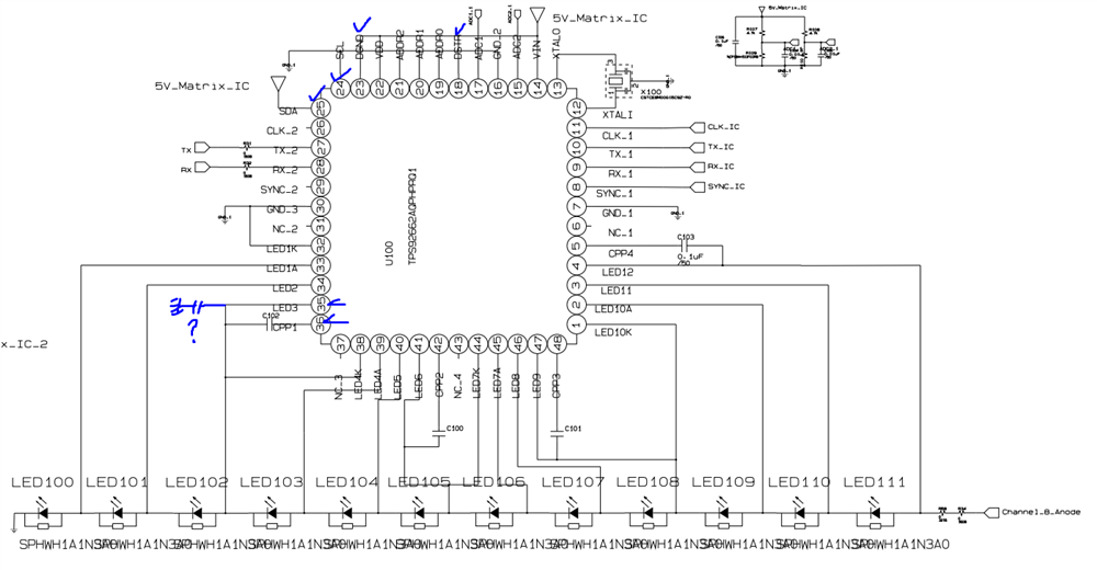
I've reviewed customers schemetic. But I have some question on several points.
SDA,SCL / DGND/ LED3&CPP1/ XTAL0

1. SCL = low, SDA = High => so, it will have 100% duty at POR (LED on). Is it right?
2. DGND is not connected with GND, but connected with Vin. Is it ok?
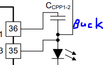
3. LED3 : "Connect to anode of LED3. Connect 10-nF capacitor to GND." Dose this sentence mean anode or GND with cap?
Or should be connected to anode and also GND through 10nF cap ?
And from the picture below, "Buck regulator output" is connected to CPP&LED line. Which case it should be?
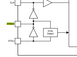
4. XTAL0 : It is difficult to understand this pin's role. Why this pin is needed?
- CPP&LED

- XTALO

Thank you.

