This thread has been locked.

If you have a related question, please click the "Ask a related question" button in the top right corner. The newly created question will be automatically linked to this question.

TPS2115A: OUT is Hi-Z, when IN2 > IN1

Part Number: TPS2115A
Other Parts Discussed in Thread: TPS2115

Hi,

We are using TPS2115ADRBR in our system to manage two power supplies (VBUS and SYSTEM_PWR). We have followed the Auto-Selecting for a Dual Power Supply Application given on the datasheet.

PFA.,, Our Design for Power Management using TPS2115ADRBR

Also we have not used the Feedback resistor (R156). 

For D1 is connected to GND, D0 is 'NC', Please find below table for the input and output voltages.

IN1
IN2
OUT
4.5V 0V 4.5V (IN1)
0.88V 3.6V 1.68V
4.5V 3.7V 4.5V (IN1)
0.89V 5V 1.69V
0V 3.7V 1.68V

ie) Whenever IN2 > IN1, We did not get OUT from IN2 but as Undervoltage (~1.68V).

So we placed feedback resistor (R156), then we tested the iterations of input as above table. But we got the same outputs. 

Please assist us in this regard. How to make IN2 as OUT, when (IN2 > IN1)?

  • Hello, 

    I am not able to see your schematic clearly; could you send a higher resolution image or pdf?

    Best Regards, 

    Elizabeth 

  • Hi Elizabeth,

    Sorry for the inconvenience.

    PFA., Our Power Mux Circuit.pdf

    Thanks & Regards,

    Balaji G.

  • Hi Balaji, 

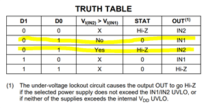
    If you are hoping to accomplish autoswitching to connect OUT to the higher of IN1 and IN2, I would recommend setting D0 equal to logic 1 and D1 equal to logic 0 rather than keeping D0 floating. This will allow you to operate in this section of the TPS2115 truth table:

    If you tie D0 to a voltage greater than 2V, do you still see this issue?

    Best Regards, 

    Elizabeth

  • Hi Elizabeth,

    Thanks for the response.

    Should the D0 be connected to a continuous voltage or for a period of time (if so, what is the time period)?  

    I just want to clarify this because the reference circuit in the datasheet also mentions that D0 as' NC'.

    Please provide your valuable inputs.

    Thanks & Regards,

    Balaji G.

  • Hi Balaji, 

    Apologies on the miscommunication, the D0 can be floating since there is an internal pullup on the pin. 

    To route out your issue, could you provide scope shots of VIN1, VIN2, Vout, and Iout during the switchover when you are seeing 1.68V on the output?

    It is possible the device is either hitting the current limit or due to the high current limit close to the maximum output current capability of the device, the device could be hitting thermal shutdown and turning off and on. If you are hitting thermal shutdown, if you were to take the average value of the output rather than the transient values, it would make sense that you are seeing around 1.68V on average. 

    A few more questions:

    • Is this 1.68V DC over a long period of time?
    • What is the total load at the output of the device?

    I would recommend removing the feedback resistor R156 as it is not needed.

    Best Regards, 

    Elizabeth 

  • Hi Elizabeth,

    1.68V is the output voltage that we observed continuously whenever IN2 > IN1. Our maximum load rating is 5.5V, 1.5A.

    I will share the scope shots, but before that, I would like to clarify another thing.

    Please find the below document.

    Components-on-Input-side-of-PMUX.pdf

    As mentioned, D16 is 'DNP', Q4 and D18 are used. No other components are available on the power supply lines of SYSTEM_PWR & VBUS.

    Can it be the reason for the under voltage or priority failure of PMUX?

    By the way, thanks for your response to my other question.

    Thanks & Regards,

    Balaji G.

  • Hi Balaji, 

    Without seeing the scope shot of how IN1, IN2, Vout, and Iout are acting during the switchover when you are seeing 1.68V on the output, it is difficult to comment on what could be the route cause. 

    Is there a possibility IN2 is simply at 1.68V?

    Are there any other connections in the schematic to the SYSTEM_PWR node?

    Best Regards, 

    Elizabeth 

  • Hi Balaji, 

    Just checking in, do you have an update here?

    Best Regards, 

    Elizabeth 

  • Hi Elizabeth,

    Sorry for the belated response.

    Due to the sudden unavailability of equipment, I couldn't share scope shots right now.

    But I would like to share some important points. When 3.6V, 50mA input supply are applied to IN2, and IN1 is 0V, the OUT from the PMUX is 3.6V.

    When 3.6V, ~15mA input supply is applied to IN2, whereas IN1 is 0VOUT from PMUX is <=1.6V.

    BQ25616JRTWR provides an input supply (SYSTEM_PWR) for PMUX.

    If you want scope shots immediately, I may need more time. If you agree, I will close this case and create it again once I can share the scope shots.

    Please share your convenience. Also, please share your inputs on my observations mentioned above.

    Thanks & Regards,

    Balaji G.

  • Hi Balaji, 

    Not a problem. So by a "3.6C, ~15mA" supply, do you mean the supply is limiting at 15mA?

    If that is the case, if your load is trying to pull more than 15mA, once the current drawn from a supply exceeds the supply capacity then the output voltage will drop. 

    That could be the issue. 

    Best Regards, 

    Elizabeth