This thread has been locked.

If you have a related question, please click the "Ask a related question" button in the top right corner. The newly created question will be automatically linked to this question.

ISO5852S: Power supply for multiple MOSFETs with different source potentials

Part Number: ISO5852S
Other Parts Discussed in Thread: UCC14240-Q1, UCC25800

Hi, 

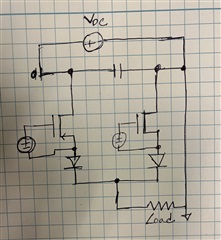
I am planning to use two SiC MOSFETs in two branches with different drain and source potentials (schematic is pasted here for reference). As the sources are at different potential due to configuration, it will impact the power supply configuration of the gate driver ISO5852S. The grounds (GND2) of the power side supplies (VCC2 and VEE2) of ISO5852S are the same, thereby essentially shorting the sources of the MOSFETs in different branches if I use same DC power supply for both MOSFETs. As this is an isolated gate driver IC, I am under the impression that the shorting of the grounds of (VCC1) at the control side will not impact the operation of the circuit.

Please suggest how to configure the power supplies for the gate driver ICs to drive the MOSFETs in two branches in the said configuration shown in the picture below without shorting the sources. Thanks in advance.

  • Hello Jonathan, 

    You're correct - you can use the same VCC1 as the primary side power supply. As of the secondary side power supply, the two gate drivers should each get its own set of bias supply, since they are connected to MOSFETs of different source potential, thus different GND2 potential. 

    You can try using a transformer driver (UCC25800 for example) and a transformer to generate secondary side bias supply for each of the gate driver, or you can try using an isolated DC-DC module with integrated transformer (UCC14240-Q1 for example) for each of the gate driver. 

    If this answers your question please let me know by pressing the green button

    Thanks, 

    Vivian

  • Hi Vivian,

    Thanks for the reply and suggestions. In case of the MOSFETs triggering at different points of time, will it be necessary to incorporate optical isolations for the PWM signals and will this scheme affect the requirement of isolation for VCC1?

    Thanks.

    Wasek

  • Hi Jonathan, 

    It should be fine if you're using two gate drivers and feeding each driver with their own PWM signal. If you want to reduce the noise on the PWM signals, you can put a small capacitor (~100pF) near the IN+/IN- pin of the gate driver. 

    Because of the capacitive isolation barrier of ISO5852S, VCC should not be affected by the two MOSFETs switching at different time. 

    Thanks, 

    Vivian