This thread has been locked.

If you have a related question, please click the "Ask a related question" button in the top right corner. The newly created question will be automatically linked to this question.

LM5109B: IC not functioning

Part Number: LM5109B
Other Parts Discussed in Thread: LM5109

I am having troubble using your product as a high side NMOS switch in my design.

High-side gate driver output does not work as stated in datasheet. The voltage on HO pin does not rise above Vin, therefore the high side NMOS is constantly partly open regardles of the PWM on HI pin. This stays the same whether I connect HI pin to GND, VCC or PWM.

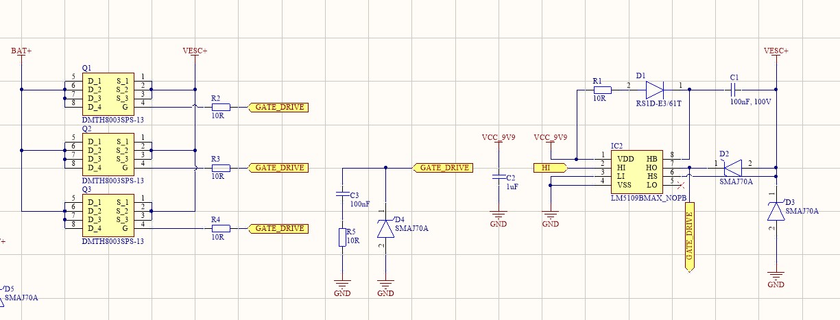
I am attaching schematic for better understanding of my design.

Please let me know if I made any error that would result in described behaviour. Also can you point me on how to troubleshoot and test you IC.

Additional question: Is it possible to use LM5109 as static switch, to drive HI pin only with static voltage and not PWM?


Note:

D2 is not placed, BAT+ (Vin) is 50V, tried with one NMOS (R2 and R3 not placed) and with 3 NMOS

Layout is made as described in datasheet, all the components are close to the IC and mosfets are 1-3 cm away.

  • Hello,

    It looks like the bootstrap circuit isn't working to generate the high-side bias here. Normally the bootstrap charges the bootstrap capacitor (C1 here) to the VCC voltage while the low-side FET is on and the SW node (VSEC+ here) goes to ground. The problem with driving the high-side only is that the bootstrap capacitor never gets a chance to charge. So you do need a low-side FET to switch for the IC to work properly.

    There are some alternatives though. One is to use a floating power supply to generate the high-side bias. Another way is to use a charge pump like shown in this document. Lastly, TI has some other products like these that work for high-side switches:

    https://www.ti.com/power-management/power-switches/high-side-switches/overview.html

    www.ti.com/.../overview.html

    These are covered by a different group though, so you would need to ask any questions to them. Lastly, I would suggest connecting the TVS/snubber circuits on your gate drive line to source rather than ground. Since everything on the high-side is referenced to the source of the top MOSFET/SW node, it makes sense to treat it as the ground of the high-side. 

    Let me know if you have any more questions.

    Thanks,

    Alex M.

  • Thanks for your reply, Is there any recommend chip for 60V, 150-200A power switch? 

  • Hello Lidong,

    There are a lot of options and different ways to go about doing that. If you want just one chip to do it then look at the efuses/hot-swap controllers I linked and sort by your requirements. It looks like there are a few that can meet them (LM5060 or LM5066 look promising). Also, the battery disconnect document shows a way to do this with a charge pump that will only require some extra components and no ICs. 

    Lastly, I should have linked this FAQ. See the section for isolated power. There are some are isolated DC/DC controllers here:

    https://www.ti.com/power-management/acdc-isolated-dcdc-switching-regulators/isolated-dcdc-converters-modules/products.html

    That could be used to easily generate a floating power supply. So, you could use this instead of a bootstrap which is duty-limited. 

    Ultimately, there is no IC from the gate driver product line that has an integrated charge pump to drive a high-side switch with 100% duty cycle. But, please consider some of these workarounds or parts from other product lines. 

    Thanks,

    Alex M.