Other Parts Discussed in Thread: CSD17579Q5A
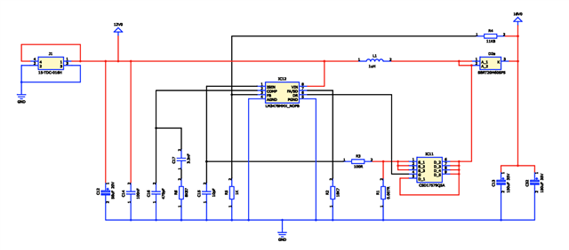
How to reduce the ripple (now 1.6V)... from the design below

I started from the design below. As stated 0.16V
Best Regards,
Piet
This thread has been locked.
If you have a related question, please click the "Ask a related question" button in the top right corner. The newly created question will be automatically linked to this question.
How to reduce the ripple (now 1.6V)... from the design below

I started from the design below. As stated 0.16V
Best Regards,
Piet
Hi Piet,
Thank you for using E2E forums, may I know your design specs Vin(max, min, typical) Vout, Iout and Fsw?
BR,
Haroon
Dear Haroon,
The specs are as stated in the WBDesign76 (pdf), but they produced the hardware as showing in schematic. Please help me to make some change that the ripple goes down...
Best Regards,
Piet
Hi Piet,
Thank you for reply. I see the design specs in the schematic, you are right. The ripple can be caused by many things, if you have followed the design instructions from WEBENCH, which I am assuming you have, the ripple could be cause by how the layout has been done, or the measuring method. Please check this TI webpage for the correct method of measuring the ripples on the output https://e2e.ti.com/blogs_/b/powerhouse/posts/how-you-measure-your-ripple-can-make-you-or-break-you
BR,
Haroon
Dear Haroon,
As you can see the production facility changed some components (due to long delivery times). I summarized it below:
Webench Design CCC_v8.2 Design
Ccomp = 2.7nF C17 = 3.3nF
Rcomp = 8.87kΩ R6 = 8.87kΩ
Ccomp2 = 560pF C16 = 470pF
L1 = 1.8µH/4.1mΩ L1 = 1.0µH/5.1mΩ
Cout = 330µF/14.0mΩ C13/C32 = 2x150µF/25.0mΩ
Can you tell me how to calculate the ripple voltage
I will measure the ripple according to the guidelines you mention in the weekend and send the results!
Best Regards,
Piet
Hi Piet,
I see, for some reason I get an error when I put your design specs in WEBENCH for LM3478. Could you please send me the waveform of the output ripple you are seeing? or are you merely simulating the design and getting the ripple in simulation? what is the load that you are getting the ripple at(light load, no load or full load)?
To answer your last question for boost devices the output ripple is heavily dependent on the ESR of capacitors, it should be low and a ceramic is a good choice for that reason with X5R or even better X7R.
With external compensation the output capacitor and output ripple formulas is consisting of two parts:


It is important that by setting an output capacitor this way we need to also check how the external compensation would need change with this new value of the output capacitor.
Hope this helps.
BR,
Haroon
Dear Haroon,
Back from holiday and starting to finalize the design...
First of all can you provide me with the document where the formulas are declared, because they refer to other like Equation 1, 2 and 6
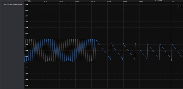
I made a screen shot of the ripple starting at full load (Peltier TEC1-12706) and then no load (open connection). The ripple is measured with a resistor divider, because the max voltage input of my analyzer (Saleae Logic 8) is 5V. The resistor divider is 220 and 680 ohm serial over the output of 16V

Best Regards,
Piet
Hi Piet,
Thank you for your reply, hope you had a great vacation. Here is the link to the document I mentioned in my earlier comments. https://www.ti.com/lit/an/slva372c/slva372c.pdf?ts=1659358184594&ref_url=https%253A%252F%252Fwww.google.com%252F
Regarding your waveform, is it possible to get some waveforms using oscilloscope and an actual 16V output, I am not sure about the logic analyzer you are using but with longer loops there is a chance that you might be picking up noise due to how you are measuring the output. As it is explained here how to correctly measure a signal using oscilloscopes. https://e2e.ti.com/blogs_/b/powerhouse/posts/how-you-measure-your-ripple-can-make-you-or-break-you
BR,
Haroon
Dear Haroon,
I am working thru the Document you send to me and one question is coming up. See below

Where can I find ILIM(min) and ILIM(max) the LM3478MMX/NOPB.
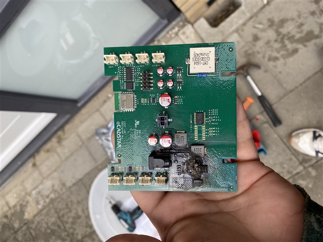
See photo below what happened.

Best Regards,
Piet
Hi Piet,
Thank you for your reply. If you look at the page 20 of the LM3478 datasheet in section 8.2.1.2.4 Setting the current limit, I think the answer to your question lies in the equation 18. I hope this helps.
BR,
Haroon
Dear Haroon,
Can you help me to get the values of ILIM(min) and ILIM(max), because I can't determinate them.
Thanks in advance
Piet
Dear Brigitte,
The document I am referring to is Application Report SLVA372C–November 2009–Revised January 2014
The boost converter is designed with WEBENCH ®. For the schematic see and report see
Best Regards,
Piet
Hello Piet,
The app note you are referring to is for calculating a power stage for a device that has the power switch integrated and then you get the values of ILIM out of the datasheet of the IC.
For LM3478, the power switch is external, so the external MOSFET has to be able to handle the calculated maximum switch current. A rough estimation can be based on the input power you need for delivering 7A at 16V. Input power is roughly 132W (VOUT*IOUT/efficiency (I used 85% as a first estimation)).
So the input current at 12V is 132W/12V = 11A, so a rough estimation of the switch current is something above 13A, as some ripple current needs to be taken into account. As I want to have some margin, I would recommend using at least a 15A, better 20A MOSFET.
Best regards,
Brigitte
Dear Brigitte,
Thanks for the explanation
In the first batch (250 pieces) we used the CSD17579Q5A!
CSD17579Q5A {30 V N-Channel NexFET™ Power MOSFETs}.pdf
Do you have an idea why the measured ripple is so high... See below for the ripple
Best Regards,
Piet
Hello Piet,
Which signal are you showing in the scope plot. Is this the output voltage? In the measurement, I can see a lot of ringing, but not a clear output voltage ripple. The output voltage ripple would be a signal in the same frequency as the switching frequency, but it seems that all signals I can observe there are at a higher frequency. This behavior is often called ringing.
If I understand your request correctly, you want to reduce the ringing. Ringing is caused by the converter switching activity and heavily dependent on the used MOSFETs. Fast MOSFETs cause high ringing. TIs MOSFETs are known for being extremely fast and therefore special care needs to be taken when doing the layout. See here: https://www.ti.com/lit/an/slpa010/slpa010.pdf
Best regards,
Brigitte
Dear Brigitte,
Thanks for information.
Our convertor is a boost convertor and not a buck convertor as described in the document called slpa010.pdf! Do we have to follow the recommendations as described in the document or can you give us the name of the document which handle the boost convertor.
Best Regards,
Piet
Dear Brigitte,
In the meantime, I was searching for a document about ringing in conjunction with a boost convertor and I found application report SLVA255 from September 2006. Is there a newer version available?
Best Regards,
Piet
Hello Piet,
Speaking about ringing caused by a MOSFET, it is extremely important to take care on a very good layout. The rules for a buck converter are not too far off of the rules for a boost converter as both power stages are the same, just input and output are exchanged.
SLVA255 has not had an update yet, but the basic physical rules did not change.
Best regards,
Brigitte
Dear Brigitte,
We were discussing a new PCB layout, but we have still a lot a stock. My question, which components we have to take of so that the boost is not operational...
Best Regards,
Piet
Hi Piet,
Thank you for your message, but I am not sure I follow. Could you repeat and elaborate your question?
Thank you
BR
Haroon
Dear Haroon,
Which components I have to take out (desolder) to disable the boost-convertor.
Best Regards,
Piet
Hi Piet,
I am also not sure what you would like to get.
If you desolder the inductor the whole boost and any pass through will be disabled but the Controller will still be switching and consume power.
If you also desolder the controller and the MOSFET this will be also gone.
If you only desolder the Controller you still have the passthrough and the output will be supplied with the input voltage level (minus Diode voltage drop).
Best regards,
Stefan
Dear Stefan,
Thanks for the clearly answers.
In the meantime, we design a new PCB layout, because we want to know what the reason was. We had a ripple of more than 1.5 V and a lot of ringing. I made a cut of the design so that you can comment the new one if you have some spare time.
There where 2 main reasons that we changed the PCB. These recommendations you can find in the document called "Minimizing Ringing at the Switch Node of a Boost converter.pdf {slva255}"

Best Regards,
Piet
Dear Stefan,
Thanks for the support and I will share the result.
Best Regards,
Piet
Hi Piet,
I have not seen an update for the last 12 days, so I assume the questions are/or answered and the issue is solved.
I close this thread now. If there is still something open reply and the thread will get open again.
If you have any other question or of the thread gets locked, please open a new one.
Clicking the Resolved Button also helps us to maintain this forum.
Best regards,
Stefan