This thread has been locked.

If you have a related question, please click the "Ask a related question" button in the top right corner. The newly created question will be automatically linked to this question.

LM3409: Flickering light output at certain duty cycles when using shunt-FET dimming

Part Number: LM3409

I'm designing a lighting application that will drive a string of 8x LEDs at 24.8V/60mA from an input voltage of 30V. I'm chosen an ROFF1 of 2KΩ, for a switching frequency of ~546khz. I'm using a 47µH inductor. and my shunt-FET has an RDSon of 0.16R. The shunt FET has a total minimum pulse time of < 20ns (turns off delay + turn off time + turn on delay + turn on time).

I've calculated my ROFF2 by choosing the minimum frequency (20khz) I want the driver to switch at in its shunted state. I've calculated this value to be 2.24MΩ, which would result in a Toff of 50µs. Since this is well below the maximum Toff of 300µs, I thought this would work. In testing my light, however, I noticed that the output starts flickering below a certain PWM duty cycle, before stabilizing at the lowest value. I investigated with my oscilloscope, but I'm having a hard time interpreting the traces in the state where the light is flickering.

This is a measurement of the switching node from the stable state:

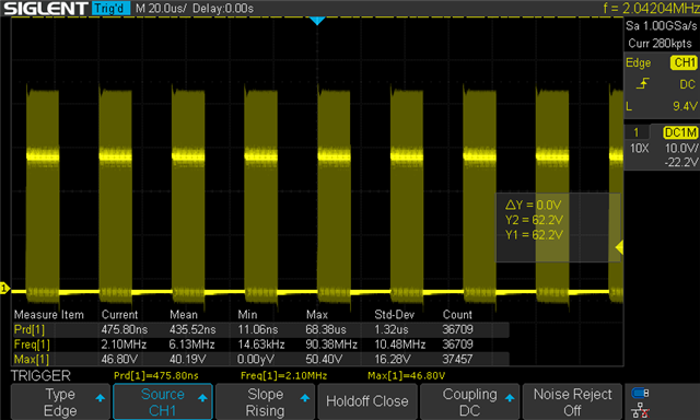
From what I can tell, this is operating as it should. The off time in this case is ~20µs, so the lower frequency operation mode driven by ROFF2 never has a chance to kick in. If I lower the duty cycle on the shunt FET PWM, I start to see this at the switching node, and the light output starts flickering:

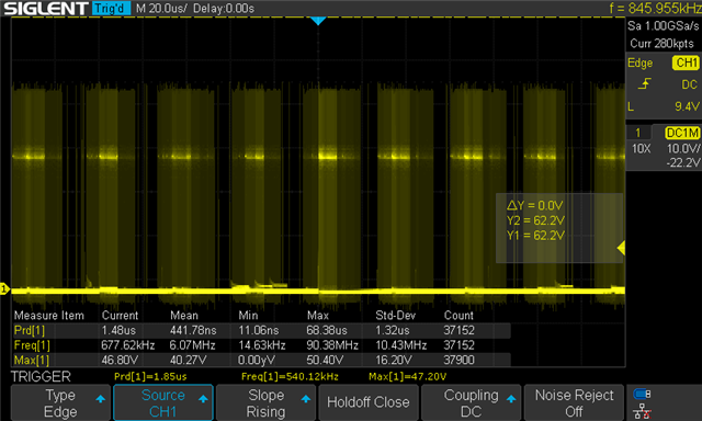
The off time is still above the 50µs limit (at 20khz) that would result in the ROFF2 frequency being in effect. It's unclear what is happening here. This transition is accompanied by instability in the light output.

Finally, if I reduce the duty cycle enough I see this:

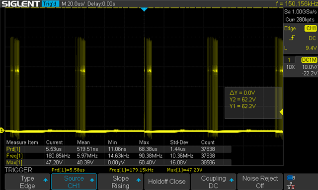
The light stabilizes here at a low output level. I believe that ROFF2 triggers a switching cycle here, since the off time is > 50µs. The overall time off is still well above the maximum off time of 300µs, so my sense is that the problem is not relative to exceeding that maximum.

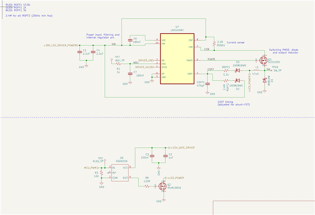
Here is a schematic of my design:
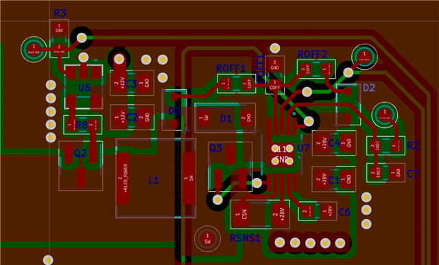
And the PCB layout:

  • Hello Alexander,

    I am looking at your layout and I believe it needs to be fixed.  Have you laid out a buck switcher before?  You haven't shown the reference designators I think I figured out the layout anyway.  Your input and output filters (especially important on input caps) have large ground loops with poor connections to your internal ground plane.  Did you use our EVM to verify how well it worked supplying your load?    I would also use that as a reference for your layout.  I have Altium files which I can share.  

    https://www.ti.com/lit/pdf/snva391 

    Here is an app note on switcher layouts.  

    https://www.ti.com/lit/an/slyt614/slyt614.pdf?ts=1659129237068 

    https://www.ti.com/lit/pdf/slua366?keyMatch=BUCK%20LAYOUT%20GUIDELINES 

    https://www.ti.com/lit/pdf/snva054?keyMatch=COMMON%20MISTAKES%20IN%20POWER-SUPPLY%20LAYOUTS%20AND%20HOW%20TO%20AVOID%20THEM 

    We can also have a meeting an go offline to go over it.  

    -fhoude

  • You pretty much hit the nail on the head, I don't have a lot of experience laying out switching power supplies. Your comment made me take a look at the ground loops in my design and as you noted I'm not making great use of my interior ground plane. Do you think this is likely the cause of the flickering?

    I would definitely be happy to go offline if you would be willing. Is the issue a matter of placing vias to make smaller ground loops that go through the interior plane, or is there something more fundamental I am missing with my design?

    Vias would help, but you could also reconfigure your part placement, remove traces that cut up your ground plane and put those less critical traces on internal planes.  What program are you using?  Maybe I can import them into my Altium and redo the placement and traces for you to show you how it should be done.  Or we can dive session.  You can request my "friendship" by hovering over my name and selecting the "request friendship" button.  There you can add your email address in the notes and I can email you a webex invite to go over the layout in real time. 

    I've added the reference designators back to my design for easier viewing (I've also added a few vias to help with the ground loop issue). I would just highlight the fact that I actually don't have any filtering on the output of the LM3409, just input filtering there and on the input for the transistor driver. The documentation for shunt-FET dimming indicated that output filter caps would interfere with the PWM signal.

    Yes, you are correct you don't want much capacitance.  I would put a little capacitance though for noise.  You can adjust later for transient response and PWM behavior.

    Thanks for the feedback.