Other Parts Discussed in Thread: TPS546D24A
Hello,
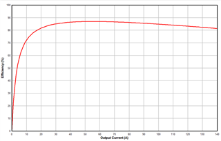
My customer has a few inquiries about the TPSM8D6C24 design along with a circuit review.
Please review the attached file below.
TI_TPSM8D6C24_design_review.pptx
Thank you.
JH
Hello,
My customer has a few inquiries about the TPSM8D6C24 design along with a circuit review.
Please review the attached file below.
TI_TPSM8D6C24_design_review.pptx
Thank you.
JH