This thread has been locked.

If you have a related question, please click the "Ask a related question" button in the top right corner. The newly created question will be automatically linked to this question.

TPS65253: Schematic review / Converter not working when configured for 5V

Part Number: TPS65253


Hi Power Management Experts,

I'm using two instances of TPS65253, can you please support with schematic review and comment on what could cause the problems observed?

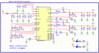
  • One of these devices is configured for 5V, however I don't have any output. When I connect the load it only shows a few mV and without a load it's 0V. I'm only using 1 of the channels, please let me know if I should treat the unused channel in a different way
  • On the other device I'm using two 3.3V outputs, In this case 3.3VD (channel 2) is having trouble sustaining the load when input voltage is larger than ~7V, please tell if I should change something to get the highest possible current output from both channels. I'm currently debugging this one to better understand the problem.

Thank you in advance for your comments, and please let mw know if further details are required for the analysis.

Best regards,
-Ivan Salazar

  • Hi Ivan,

    Thanks for reaching out. I will get back to you soon. Thanks!

    BRs

    Lucia

  • Hi Ivan,

    Sorry for late response.

    1. For device 1, could you please help measure the waveform of pin V3V and V7V, also SW pin?

    2. For device 2, could you please let me know the actual output current for both Buck1 and Buck2 ?

    Thanks!

    BRs

    Lucia

  • Hi Lucia,

    Thank you for following up, I have some updates below:

    • Measuring Device 1:
      • Pin 21 (V7V) = 0V
      • Pin 22 (V3V) = 0V
      • Pin 8 (VIN1) = 7V
      • Pin 12 (VIN2) = not connected, should this be powered even if not using the 2nd channel?
    • Regarding Device 2, we have narrowed down the problem to be some radiation form the switching waveform.
      • Performance improves if we add 140-Ohm in series with bootstrap capacitor, however at higher VIN (like 10V) the problem still arises.
      • We're planning to add 2nF+10-Ohm snubber on the switching side of the inductor. I'll update on the results later.
      • Please comment if any of the above is not recommended

    Best regards,
    -Ivan Salazar

  • Hi Lucia,

    Quick update on Device 1:

    • I shorted VIN1 to VIN2 and now I have proper 5V output from Channel 1. So this means we have to connect VIN to both channels even though Channel 2 is not used.

    We're still debugging Device 2, and plan to implement the same fixes (snubber, series resistor) on Device 1 since they're both in the same system. Please comment if you consider these fixes are not recommended or if there is another workaround.

    Thanks.

    Best regards,
    -Ivan Salazar

  • Hi Ivan,

    Sorry for late response.

    (1) Yes, you are right. We need to connect both VIN1 and VIN2 as input for TPS65253. V7V is from VIN2. Thus, if no VIN2, there will no Vcc, also no output for the circuit.

    (2) I am still checking item2. 

    Thanks!

    BRs

    Lucia

  • Hi Lucia,

    I have some updates after further debugging on device 2 (dual 3.3V output) on our side:

    • We add a series 140Ohm resistor in series with bootstrap capacitor
    • We add 1.5nF+29.4Ohm snubber on SW side of each inductor
    • After both these changes, we no longer have the radiation problem even at higher input voltages
    • However now we're facing what seems to be overheating shutdown after long operation times at Vin > 12V
      • When the board is powered from 12V, and we disconnect as many things as possible (only remain some LDOs and USB controller), it consumes about 500mA, this seems to high for idle operation. Also the PCB around the buck converters is heating considerably.
      • Do you see anything on the schematic that can suggest an increased load to the Buck converter so that it consumes so much current?

    Thank you in advance for your comments. Let me know if any clarification is required.

    Best regards,
    -Ivan Salazar

  • Hi Ivan,

    Thanks for your useful input. We will do more analysis based on your input. Really thanks!

    BRs

    Lucia

  • HI Lucia,

    Just a quick notice for the community:

    After thorough analysis of this issue we can confirm the issue was an incorrect connection on the Bootstrap capacitors, these were connected to the output of the inductor instead of LX pin side. Fixing this error on both 3.3V and 5V buck gets rid of all the problems, thus no snubber nor additional circuitry is required.

    Best regards,
    -Ivan Salazar