This thread has been locked.

If you have a related question, please click the "Ask a related question" button in the top right corner. The newly created question will be automatically linked to this question.

TPS61020 : Glitch on EN pin

Other Parts Discussed in Thread: TPS61020

Hi,

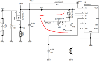
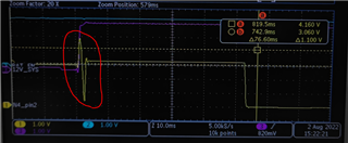
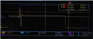
I am using TPS61020 with 3V battery VBAT voltage. Enable  pin is handled thorough external MOSFET as shown below. At start up , when I enable MOSFET V90 ( BAT_EN = 1) , I see glitch on EN pin, which is going upto 7V. This is observed at Drain of MOSFET V90. But it is not seen at Anode of V88. What can be the reason for this ? whether this is acceptable ? How this can be avoided ?


  • Hi Prafulla,

    Thanks for reaching out.

    I have some questions about this.

    1. Since V90 is PMOS, and VBAT is already for example 3.3V, maybe we should set BAT_EN=0 but not 1 to enable the device?

    2. From the waveforms, I see BAT_EN is a stable 3.2V, what is N4_pin2?

    Regards

    Bryce

  • Hi Bryce, 

    Yes you are right. Now I have attached correct waveform to refer. Test condition is, when BAT_EN is going high ( Disable the TPS61020 IC),  TPS_EN goes low and then MCU pin forcefully again takes TPS_EN high for some time. but during this sequence, positive peak on TPS_EN is not expected.

    How it can be avoided ? What can be the reason for it ? Is there any reliability issue to IC because of this ? Sometimes this peak is reaching upto 7V as well. 

  • Hi Prafulla,

    What is the state of TPS_EN when BAT_EN is going high? MCU outputs low or high?

    Can you also probe the voltage of P248(source of the mos)?

    Regards,

    Bryce

  • HI Bryce,

    As shown in waveform, yellow waveform is of TPS_EN & pink one is BAT_EN. So when BAT_EN goes high, TPS_EN goes high ( glitch) and then it goes low. Ideally it should go low without any glitch.I probed P248 as well. It shows the same glitch as TPS_EN. 

    TPS_EN is controlled by MOSFET & also by MCU directly ( P73 net ). So MCU makes EN high sometime after BAT_EN goes high. 

    Regards,

    Prafulla S.

  • Hi Prafulla,

    The waveform on TPS_EN is like the oscillation caused by sudden turn-off of V90. Have you tried add 1.0uF cap between EN and GND?

    Regards,

    Bryce

  • I tried with placing cap of 10nF, it completely reduces spike but it also causes slight increase in battery current consumption which I can not go ahead with. Also, increased value of cap will impact, TPS_EN going high because of capacitor charging time. My theory is, flow of glitch is from TPS_EN to drain of V90 and from body diode , it is to source of V90. But not sure, how it can be avoided. 

  • Hi Prafulla,

    Can you add a 3.3V Zener diode between EN and GND to reduce spike? 

    Regards,

    Bryce