This thread has been locked.

If you have a related question, please click the "Ask a related question" button in the top right corner. The newly created question will be automatically linked to this question.

LM5141: With LM5141 output 12V/10A high power, the switch frequency is 2.2M

Part Number: LM5141
Other Parts Discussed in Thread: LM5146, CSD17308Q3, CSD18532Q5B, CSD18534Q5A

Hi every expert, my design is as below.

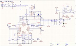
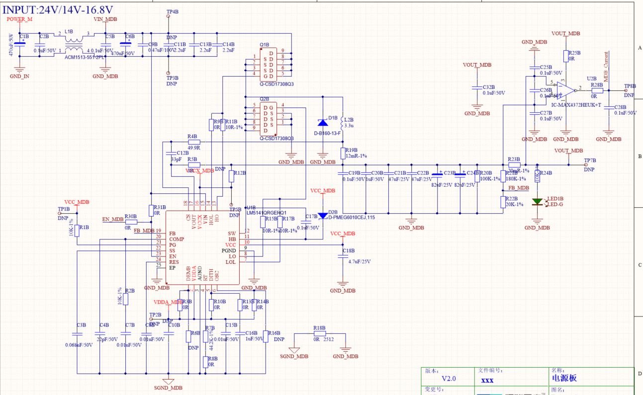
LM5141QRGERQ1  design:

     switch power supply: input 24V

    battery supply:14V-16.8V

     output voltage12V,output current need  10A,

     power inductor:  Air core inductor 3.3uH

    Fsw=2.2MHz

    DEMB-VCC,FPWM mode

     I want to know if my design is ok to have output 12V/10A with above design.

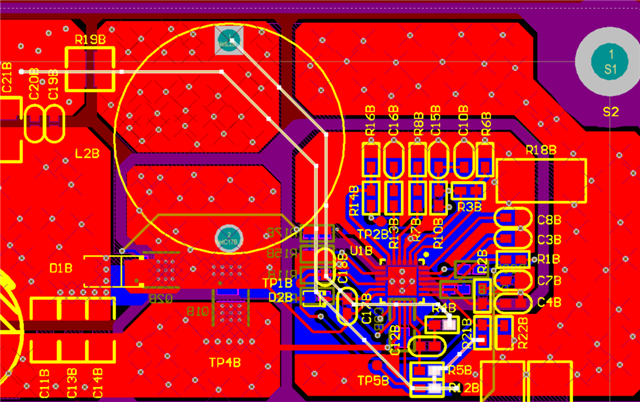
Now I can get output 12V/3.5A when R19B is 12mΩ,while when R19B is 0Ω the output current can reach 5A.

My question is if I want to get stable 12V/10A, what can I do?

I am glad to get a good answer.Thank you.

  • Hi Baron,

    Please use the LM5141 quickstart calculator to assist with component selection this design (see the product folder for a link to download).

    R19B is the current sense resistor, which is required for current-mode control (do not use 0mΩ). Also, I don't recommend using an air-cored inductor. As a starting point, take a look at the LM5146 EVM, which is 12V/8A/400kHz.

    2.2MHz is quite high here, leading to high switching losses - 400kHz is preferable from an efficiency/size tradeoff standpoint.

    Regards,

    Tim

  • Hi Tim:

    I am glad to receive your intelligent reply promptly.Thanks a lot.

         First, I want to say the circuit based on LM5141 is used in a particular situation with high-intensity magnetic,and the highest magnetic is 3T.So I have to use an air core inductor,if you can recommand another kind of inductor working in high-intensity magnetic will be perfect.

    I have downloaded the quickstart tool,and tried to calculate every electric parameter.

         Also to avoidding affect the working frequency 64MHz/128MHz of MRI, I make the LM5141 work at frequency of 2.2MHz.And the high switching frequency need small size/inductance value air core inductor is a reason I secleted 2.2MHz as the switching frequency.

        Switching Frequency,Fsw:2.2MHz          Recommand Inductance:1.36uH

        Switching Frequency,Fsw:1.8MHz          Recommand Inductance:1.67uH

        Switching Frequency,Fsw:400KHz          Recommand Inductance:7.5uH

    I will right now download the LM5146 EVM and make a particular analysis.

      Thank you again.

    Best reagrd.

    Baron.

  • Hi Baron,

    I recommend using a shielded inductor, for example the Cyntec part used in the LM5146 EVM. There are some alternatives given in the datasheet apps examples.

    Regards,

    Tim

  • Hi Tim,

         Q1:

    As below,the highlight wire is the signal of between sense  resistor R19B-pin1 and R19B-pin2.The L2B is the inductor.The problem is signal wire got through below at inductor.And the waveform of yellow is the G to GND_MB of Q1B,the waveform of blue is the G to GND_MB of Q2B.Obviously,the waveform is not very good.My question is "If the signal wire got through below at inductor is the primary cause generated the bad waveform?"  "And if the  signal wire got through below at inductor is the primary cause that the output current can not reach more than 5A?"


    Q2:

        I am not sure the MOSFET I choosed CSD17308Q3 is approprite,Qg is 3.9nC.When I set the Fsw as 2.2MHz,the smaller Qg is better,right?

        When the high-side MOS and the low-side MOS used CSD17308Q3(Qg=3.9nC),the output current can reach 3A.

        When the high-side MOS  used CSD17308Q3(Qg=3.9nC)  and  the low-side MOS used SQ7414AEN-T1-GE3(Qg=16nC,LM5141 EVM used this MOS),the output current can reach 5A or more.

        I want to know what is the root cause produce the different output current?

    Q3:

        When the circuit worked with a big load,for example the output current is 5A,the temprerature ot the MOS will reach 70℃ or more,is it a normal phenomenon?And if I used a large size of MOS--SON 5x6mm will better.

    Q4:

        If I want to get a big current about 10A and also considerring the thermal design problem.As below,which MOS is beeter?

    1)CSD17308Q3——VSON 3.3mmX3.3mm,

    2)SQ7414AEN-T1-GE3——VSON 3.3mmX3.3mm,used in LM5141 EVM

    3)CSD18532Q5B——SON 5X6mm

    4)CSD18534Q5A——SON 5X6mm

    5)NVMFS6B14NLT1G——SO-8F,used in LM5146 EVM

    6)NVMFS6B25NLT1G——SO-8F, used in LM5146 EVM

    Thank you again.

    Best reagrds.

    Baron.

  • Hello Baron,

    A1 response to Q1, its hard to say what the primary reason is, as there appears to be a number of potential improvements that can be made in the design and rerouting the things referred to would be significant in terms of improvements. 

    A2 response to Q2. Smaller Qg is better in terms of improving efficiency by reducing transitional losses.

    A3 response to Q3.  Yes the temperature of the MOSFET will increase as the I^2 x RDSon increases with load.  A larger sized MOSFET package will allow the heat to conduct better reducing the temperature rise of the MOSFET.

    A4 response to Q4.  Suggest using the QS tool to calculate the losses of each FET, but the general rule is the lower gate charge results in lower transitional losses and the lower RDS on results in lower conduction losses.

    Hope this helps?

    David.