This thread has been locked.

If you have a related question, please click the "Ask a related question" button in the top right corner. The newly created question will be automatically linked to this question.

TPS62827: Bode Plot

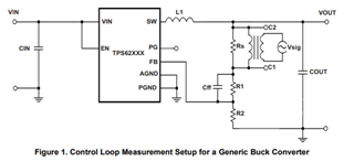
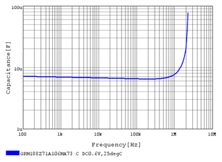
Part Number: TPS62827

Hi


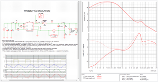
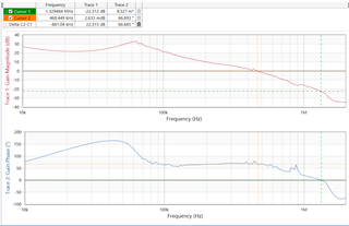
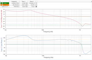
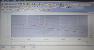
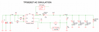
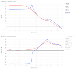
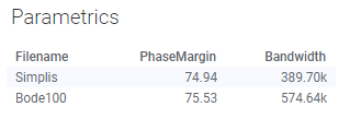
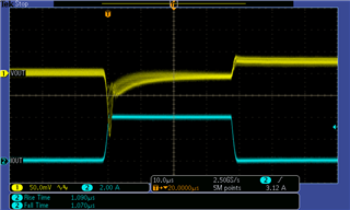
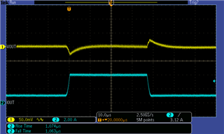
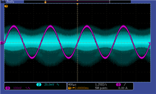
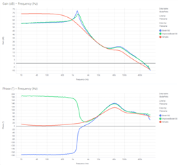
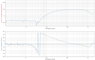
I cannot find the stability simulation tool as Bode Plot in the WEBENCH POWER DESIGN,

Could you please help to check whether this application is feasible?


We are going to evaluate the suitable network of voltage divider other than the typical one as datasheet discoursed.


Regards

Ben

  • Hi Ben,

    I am taking care of your request and will provide you feedback by tomorrow at latest.

    Have you tried the simplis model already? 
    www.ti.com/.../slvmdi7

    Best regards,
    Nelson

  • Hi Ben,

    I was able to run simulations with the Simplis AC Model for the TPS62827 found in here:
    https://www.ti.com/lit/zip/slvmdi7

    Solid line - C3=120pF
    Dotted line - C3=20pF

    Do you have software capable of using this AC Model?
    If not, then could you provide me the values for the resistor divider network and the BOM that you would like to evaluate?
    I could run the simulations and provide you the results.

    Best regards
    Nelson

  • Hi Nelson


    Thanks for the quick reply!

    I was trying to find the Simplis with a trial version,

    Unfortunately, the restriction leads to the simulation abort

    We decided to make the real measurement instead at this moment and may request a couple of cases of simulation to correlate with the measurement


    Two additional questions were raised as follows


    • The typical application circuit in the datasheet is the best suit and strongly recommended, if the replacement of the inductor, output capacitors even the voltage divider to FB are required, what is the simple principle we must follow? Could you please explain with a simple example?


    • According to the schematic, the loop is broken and injected the signal at FB which is much different from the traditional buck converter breaking the loop and injecting the signal at the upper of the voltage divider, should we follow the schematic while making the real measurement? What is the intended break then injection for?


    Regards

    Ben


  • Hello Ben,

    Regarding your additional questions:

    1. Design of L, Cout and Cff

    What are the parameters you want to optimize by changing L, Cout, Cff?
    - Efficiency?
    - Vout ripple?
    - Banwidth?
    - Area?

    The internal circuitry is configured around L=470uH, C=3x10uF. Changing the inductor value is therefore not recommended.
    TI evaluated the stability with Nominal Cout up to 100uF. 

    For design recommendations, you could refer to the formulas in chapter 9 of the datasheet.

    e.g.:

    You can change (reduce) the resistor divider values but this would lower the efficiency for light loads.
    Cff would be a function of R2 as indicated by formula (5). This is critical for stability.

    As a conclusion, If you definitely want to change L and Cout, it would be a very recommended to evaluate your solution on the EVM.

    2. Bode plot measurement

    You are right, including extra hardware on the FB is not recommended and this is only a method used for the Simplis simulation.
    The setup we normally used is the following:

    Best regards

    Nelson

  • Hi Nelson


    Thanks for the recommendation!

    Regarding Bode Plot measurement, could you please deliver a response curve of the lab test? We may try to correlate the result with EVM as a quick start


    Regards

    Ben

  • Hi Ben,

    is there a particular set of conditions that you would like to evaluate?

    e.g.

    Vin = 5V
    Vout = 1.8V
    Iout = 4A
    Cout = 3 x 10uF

    Best regards
    Nelson

  • Hi Nelson


    We expect to set the following applications up


    VIN = 3.3V / 5V, VOUT = 0.6V, L = 0.47uH / 1uH, COUT = 10uF x 3, IOUT = 4A


    It is welcome to the recommendation for our expectations.


    Regards

    Ben

  • Hello Ben,

    Thanks for the test conditions.

    We expect to run this test by end of this week. We'll let you know as soon as we have the results.

    Best regards
    Nelson

  • Hi Ben,

    Let me respond to your request as Nelson is out of office for few weeks. I did the bode plot measurements for TPS62827 for the test conditions you provided. Please find attached report for the same. 

    0.47uH, 3.3V_TPS62827.pdf1uH, 3.3V_TPS62827.pdf

    Let me know in case of any further questions.

    Thanks a lot!

    Best regards

    Sneha

  • Hi Sneha


    Could you please show me the result directly according to the curves you provided?

     I did not quite understand the intended cursor @ specified point


    L = 0.47uH

    L = 1uH

    Bandwidth (kHz)


    Gain Margin (dB)


    Phase Margin (Degree)


    Thanks

    Regards

    Ben

  • Hi Ben,

    I will get back to you tomorrow on this request.  

    Best regards

    Sneha 

  • Hi Ben,

    Please see below for the results.

    With 0.47uH: BW = 636.02 kHz, GM = - 59.2dB, PM = 67.931 degrees

    With 1uH: BW =  494.1 kHz, GM = -63.61dB, PM = 74.775 degrees

    Regarding the PM, the system looks stable. However, the negative GM does not look reasonable to me. Please let me re-confirm this value and update you tomorrow.

    Thanks!

    Best regards

    Sneha 

  • Hi Sneha


    Thanks for the reply!

    According to the plot of phase, does it experience a phase shift beyond 180 degrees as the frequency sweeps from 100Hz to 1MHz?

     It looks much different from the conventional response curve.


    Regards

    Ben

  • Hi Ben,

    I reconducted the measurements now. The GM did not look reasonable to me earlier. I apologize for the inconvenience. 

    Please see below images for the new bode plot results:

    1) 0.47uH: PM: 66.7degrees, GM: 22.315dB, BW = 541.23kHz

    2) 1uH: PM: 75.16degrees, GM: 35.613dB, BW = 360.8kHz

    Thanks a lot!

    Best regards

    Sneha 

  • Hi Sneha


    Could you please help to double-check the curve swept from 100Hz to 10kHz as well?

    I really concerned about the low-frequency part since the behavior of that range is out of my understanding.

    Does it indicate that the system is unstable from 100Hz to 10kHz?


    Any comment is welcome!


    Thanks

    Regards


    Ben

  • Hi Ben,

    Internal control loop acts in the low frequency region. Whenever the phase crosses the +/-180 degrees, the internal control loop acts and tries to compensate for the phase, that's why you observe the jump in the phase. 

    We are generally concerned in the higher frequency ranges 10k-2MHz, where the buck control loop is active and it defines the stability of the system. The phase margin > 45 degrees states that the system is stable and I do not see any concern with this application. 

    Thanks a lot! 

    Best regards

    Sneha

  • Hi Sneha


    Thanks for the behavior description!

    May I conclude that we should only focus on the frequency range near the bandwidth, even if the low-frequency response “looks weird”?


    Regards

    Ben

  • Hi Ben, 

    Yes  that's correct. We only consider phase margin and  gain margin to check for stability.

    Thanks!

    Best regards

    Sneha 

  • Hi Ben,

    Do you have any further questions here? If not, please feel free to close this thread by clicking "Resolved" button.

    Thanks!

    Best regards

    Sneha

  • Hi Sneha

    I briefly make the measurement of the Bode Plot using EVM

    The condition is as follows


    VIN = 3.3V, VOUT = VREF = 0.6V, L = 0.47uF, COUT = 10uF x 3, IOUT = 4A


    Sneha

    Ben

    PM (Degree)

    66.7

    80.865

    GM (dB)

    22.315

    18.021

    BW (kHz)

    541.23

    296.47


    Unfortunately, I cannot make a good correlation with your result.

    Do you have any recommendations guiding me for the optimized measurement?


    Thanks

    Regards


    Ben

  • Hi Ben,

    I am not quite sure what could possibly be the reason for this.

    Could you please share a picture of your measurement setup? Did you use the Network analyzer or a Bode 100 for the measurements? Also, could you share the test settings used for your measuremet? Overall, by looking into the results, there does not seem to be unstability issues with the application.

    Thanks!

    Best regards

    Sneha

  • Hi Sneha


    The equipment we used for the Bode Plot is Model 300 30MHz Frequency Response Analyzer manufactured by AP instruments inc.


    Since the measurement is briefly made, I have to reproduce the curve again and record the test setting simultaneously; maybe I can also earn another one for the condition as the simulation result of the first time Nelson delivered.


    Could you please run the simulation for the following conditions besides the actual measurement?

    VIN = 3.3V, VOUT = VREF = 0.6V, L = 0.47uF, COUT = 10uF x 3, IOUT = 4A


    We expected to figure out what is the correlation between simulation and measurement.


    Thanks

    Regards


    Ben

  • Hi Ben,

    As Nelson is back to office now. I will let Nelson comment on your following queries. 

    Thanks a lot!

    Best regards

    Sneha

  • Hello Ben, 

    Since you were trying tomatch simulations and measurements, I had to improve the modelling of the LC filter elements.

    There is an inductance decrease that depends on IL. For IL=4A, we get aproximately L=0.4uH. (see plot below):

    https://www.murata.com/en-global/products/productdetail?partno=DFE201610E-R47M%23

    And regarding the 10uF capacitors, they have an effective capacitance of around 6uF if we see the following data from the vendor:

    https://ds.murata.co.jp/simsurfing/mlcc.html?reqtype=open_parts&partnumbers=%5B%22GRM188Z71A106MA73#%22%5D&oripartnumbers=%5B%22GRM188Z71A106MA73#%22%5D&graphop=mainall&focuspartnumberonlist=true&lcid=en-us

    This is finally the schematic used in Simplis, which also represents the BOM populated on the EVM:

    And the results of simulation and measurement plotted together:

    In summary:

    The phase margin values are very close and indicate that this configuration results in a stable system.
    Regarding bandwidth, values might seem to be way too far from each other. We know that this is difficult to achieve because of the external factors that make the L and Cout deviate from their nominal values (tolerances, VOUT and IL bias).

    Please let me know if this assessment was useful for your purposes.

    Regards 
    Nelson

  • Hi Nelson

    Thanks for the detailed description; it is very helpful to me.

    According to the modified schematic, the lower of the voltage divider R4 = 100k ohm is still connected, but I removed it as measuring the Bode Plot, what is

    the role of R4 played since the VOUT tied to FB also gets VREF as well?

    Is it necessary?


    Presently, there is still a mismatch between simulation and measurement, and seems to be very difficult to achieve a better correlation.

    Whether the alternative to the correlation is executing the load transient?

    Could you please deliver the waveform if possible?


    Thanks

    Regards

    Ben

  • Hello Ben,

    You're right. R4 is not necessary anymore. I should have removed it. It does not affect the measurement results significantly. It acts as an additional load of 6uA, which is negligible. 

    I could definitely provide the load transient waveform. However, I would like to understand your design goal and restrictions.

    What would you like to achieve by modifying the resistor network?
    What is the load step and the allowed drop on Vout for your application?

    With the EVM and a network analyzer, you can evaluate your design for stability. If the phase margin is greater than 45°, your system is stable.
    The bandwidth would tell until which frequency the converter can act and define your transient performance.

    Now back to the conditions for the low transient. Are these ones good for you?:

    VIN = 3.3V,
    VOUT = VREF = 0.6V,
    L = 0.47uF,
    COUT = 10uF x 3,
    IOUT = 0 to 4A,
    Rise/Fall Times = 1us

    Best regards
    Nelson

  • Hi Nelson

    Thanks for your deep consideration of our application!

    Q: What would you like to achieve by modifying the resistor network?

    A:

    We started from the datasheet of the TPS62827 and take typical application VIN = 5V, VOUT = 1.8V as a reference, the target is VOUT = 0.6V this time.

    Q: What are the load step and the allowed drop on Vout for your application?
    A:

    According to the waveform shown in the datasheet, the output drop is about 50mV with the application VIN = 5V, VOUT = 1.8V, IOUT = 1 ~ 2A

    After calculation, the percentage = 50mV / 1.8V *100% = 2.78%

    For VOUT = 0.6V, we expected the load transient is not worse than the result of the typical application VOUT = 1.8V

    Nelson:

    With the EVM and a network analyzer, you can evaluate your design for stability. If the phase margin is greater than 45°, your system is stable.

    The bandwidth would tell until which frequency the converter can act and define your transient performance.

    Ben:

    How fast the load step can reflect the bandwidth limitation? Is it associated with the ringing? The conventional electronic load is unable to generate the fast step, could you please help identify the system bandwidth with a suitable load step?

    Nelson:

    Now back to the conditions for the low transient. Are these ones good for you?:

    VIN = 3.3V,
    VOUT = VREF = 0.6V,
    L = 0.47uF,
    COUT = 10uF x 3,
    IOUT = 0 to 4A,
    Rise/Fall Times = 1us

    Ben:

    Yes, this case above is OK, we also need to understand the operation under CCM to CCM transient

    Could you please provide additional cases as references?

    I listed the request as follows


    VIN (V)

    VOUT (V)

    IOUT (A)

    L (μH)

    COUT (uF)

    Load Step @ Rising / Falling (μs)

    3.3

    0.6

    0 to 4

    0.47

    10 x 3

    1

    3.3

    0.6

    1 to 4

    0.47

    10 x 3

    1

    5

    0.6

    0 to 4

    0.47

    10 x 3

    1

    5

    0.6

    1 to 4

    0.47

    10 x 3

    1

    5

    1.8

    0 to 4

    0.47

    10 x 3

    1

    5

    1.8

    1 to 4

    0.47

    10 x 3

    1


    Regards

    Ben

  • Hi Sneha,

    I meet the same phase curve when perform other devices Gain/Phase test. How to understand “Internal control loop acts in the low frequency region” ,Why does it make phase jump and make gain a peak?  

  • Hi Ben,

    Below you will find the required load transients. I will carry on with my response to your other comments tomorrow.

    Single Multiple
    3.3Vin 0.6Vout Iout 0 to 4A x
    3.3Vin 0.6Vout Iout 1 to 4A
    5Vin 0.6Vout Iout 0 to 4A x
    5Vin 0.6Vout Iout 1 to 4A
    5Vin 1.8Vout Iout 0 to 4A
    5Vin 1.8Vout Iout 1 to 4A

    Best regards
    Nelson

  • Hello Ben, thanks for your patience.
    I hope the collected transients helped you find conclusions about your design.
    It is important to know the slew rate of IOUT before comparing the results I provided with the ones of the datasheet.
    A faster IOUT rising would mean a bigger drop on VOUT. That's why it's important to know how fast you need to deliver IOUT.

    I collected a series of materials that discuss the relation between load transient and converter bandwith. There are some formulas that relate both but as explained in the video series, they are approximations. The current approach is to design to meet a target impedance:

    how-to-determine-bandwidth-from-the-transient-response-measurement

    https://training.ti.com/understanding-transient-response-time-and-frequency-domain
    https://training.ti.com/output-capacitor-selection-using-target-impedance-approach?context=1139912-1139915
    https://training.ti.com/dc-load-lines-how-they-can-benefit-your-next-design?context=1139912-1139916

    Best regards,
    Nelson

  • Hello Zhihua,

    These untypical phase shift can be explained by the low SNR of the CH1 signal (Voltage at FB in cyan) while measuring the Bode Plots in low frequency regions. CH2 in magenta is VFB+Sinusoidal Disturbance:

    The signal is modulated by high frequency noise coming from the switching and the parasitics of the output capacitors.
    It is difficult for the VNA or FRA to extract the low frequency component and define the phase.

    With an improved setup and better cables we were able to get a more reasonable Bode Plot, see the green curve:

    The peaking at low frequencies is related to a high Q pole, which is probably part of the compensator transfer response.
    Having a higher gain means that the system is better at rejecting disturbances.

    I checked the output impedance of the converter at lower frequencies. Output impedance relates the voltage and current at the output of the converter.
    At low frequencies Vout and Iout are in phase. After the low frequency pole between 3kHz-5kHz, Vout goes to a phase shift of 180 degrees w.r.t. Iout. 

    Best regards
    Nelson

  • Hi Nelson


    Thanks for the generated load transient as requested!

    It is beneficial to us!

    VIN (V) VOUT (V) IOUT (A) L (μH) COUT (uF) Load Step @ Rising / Falling (μs) Output Deviation (%)
    3.3 0.6 0 to 4 0.47 10 x 3 1 8, 16
    3.3 0.6 1 to 4 0.47 10 x 3 1 4, 8
    5 0.6 0 to 4 0.47 10 x 3 1 8, 16
    5 0.6 1 to 4 0.47 10 x 3 1 4, 8
    5 1.8 0 to 4 0.47 10 x 3 1 9, 3
    5 1.8 1 to 4 0.47 10 x 3 1 1.4

    If the expected output deviation should be kept at about 2~ 3% as VOUT = 0.6V, may we install additional output capacitors?


    In addition, another post shows the improved Bode Plot.

    How do you get it improved?

    Maybe I can try this way next time.


    Thanks

    Regards

    Ben

  • Hello Ben,

    Exactly. One option would be to increase the value of Cout. Keep in mind that it should be within the ranges recommended in the datasheet.

    The conditions for the load transients above are very extreme. Your final load might have less drastic Iout changes. I would spend some effort characterizing the load requirements. 

    Regarding the improvement bode plots, we recommend to use:
    - short coax cables,
    - an electrolytic bulk capacitor at CIN
    - 10Ω injection resistor
    - variable injection level
    - pure resistive loads

    Best regards
    Nelson

  • Hi Nelson

    Thanks for the great support!

     As mentioned, you would spend some effort characterizing the load requirements.

    Whether the effort is to control the current slew that could meet our specification 2 ~ 3% @ VOUT?

    In addition, I briefly listed the difference in taking the measurement

    Nelson's Recommendation Ben  what is the benifit to the recommendation ?
    short coax cables passive probe  
    an electrolytic bulk capacitor at CIN No additional CIN, keep EVM as the initial   
    10Ω injection resistor 20Ω injection resistor (Conventionally ?)  
    variable injection level variable injection level, Yes! Only a simple trial but have no idea what the reasonable size is Consideration to the better SNR ?
    pure resistive loads Electronic load under the constant current mode  

    Could you please comment briefly?

    Regards

    Ben

  • Hello Ben,

    Let me rephrase my last response. I offered to do the load steps with rise/fall times of 1us because this parameter was not mentioned in your request. This was an arbitrary value. It would be helpful to get more information from the datasheet of the MCU or processor you are powering with the TPS62827X. Your load might not require 4A/us slew rates but rather 500mA/us and relaxing this parameter would definitely improve the Vout behavior.

    Another idea to improve the load transient would be to select a part which always operates in Forced-PWM. This change would improve especially the test cases with Iout starting from 0A. However, you would be consuming some mA at no load operation.

    Regarding your queries:

    Ben Nelson's Recommendation Benefit
    passive probe short coax cables x1 passive probes are also good. With the coax cable you can get a very small ground loop and therefore reduce the coupling of external noise.
    x10 probes are not recommended because they attenuate the signals significantly.
    No additional CIN, keep EVM as the initial an electrolytic bulk capacitor at CIN Less Vin variation and therefore a power supply which is closer to be ideal. 
    20Ω injection resistor (Conventionally ?) 10Ω injection resistor Both of them are good values. The 20Ω resistor will transfer a bigger disturbance to the feedback loop, but the size of the disturbance can be reduced with the injection level. 
    variable injection level, Yes! Only a simple trial but have no idea what the reasonable size is variable injection level Consideration to the better SNR?
    - Yes, exactly. At low frequencies, the noise on the FB (CH1) might overlap the information of the sinusoidal response.
    Electronic load under the constant current mode pure resistive loads Electronic loads have a control loop to keep Iout constant and this might generate a distortion on the bode plots. 

    Regards
    Nelson