This thread has been locked.

If you have a related question, please click the "Ask a related question" button in the top right corner. The newly created question will be automatically linked to this question.

TPS51116: Through holes on the PCB thermal land pattern should be filled with resin or not?

Part Number: TPS51116

Hello,

My customer is using 20-Pin HTSSOP package.
The drawing on page 47 of the data sheet shows a gap between the back of the package and the PCB.
To ensure that the rear thermal pads are soldered to the PCB land pattern, should the through holes on the PCB land pattern be filled with resin so that no soldering from the through holes flows to the back of the PCB?

Best regards,

K.Hirano

  • Hello Hirano,

    The drawing on page 47 of the data sheet shows a gap between the back of the package and the PCB.

    There should be no gap between the back of the package and the PCB. The thermal pad should be soldered directly to the PCB.

    To ensure that the rear thermal pads are soldered to the PCB land pattern, should the through holes on the PCB land pattern be filled with resin so that no soldering from the through holes flows to the back of the PCB?

    No, filling the via holes with solder should not be necessary. Here is TI's recommendation for ensuring solder flow through the vias is not significant:

    Link to full package info: www.ti.com/.../slma002h.pdf

    Thanks,

    Travis

  • Hello,

    The thermal land of the PCB is connected to ground plan for better heat dissipation. The holes on the PCB land pattern are at GND potential. I do not see a problem with solder flow. This document explains the thermal pad soldering PowerPADTm Thermally Enhanced Package (Rev. H) (ti.com)

    Regards

  • Travis, Mahmoud,

    Thank you for your responses.
    I have one confirmation.
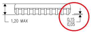
    Looking at the following drawing on the datasheet, my customer thinks that there is 0.05 to 0.15mm gap between PCB and thermal pad as circled in red.
    But, their understanding is wrong? 

    Best regards,

    K.Hirano

  • Hello Hirano,

    Apologies for the confusion. There is a very thin gap (the 0.05 to 0.15mm you mentioned) between the thermal pad & the PCB to allow space for solder paste applied by the stencil. After soldering, the gap is filled with solder (from the solder paste applied by the stencil) which forms a good thermal connection to the thermal pad. More information is in page 11 of the document in the previous link.

    Thanks,

    Travis