Other Parts Discussed in Thread: TPS544C25, TPS544B25, TPS546C20A
Hello,
In the Layout Example section of the TPS546D24A datasheet, there is an un-named purple plane. Could you please advise what this plane is?

Thank you,
Kyle
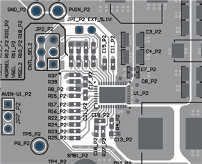
Hello,
In the Layout Example section of the TPS546D24A datasheet, there is an un-named purple plane. Could you please advise what this plane is?
Thank you,
Kyle