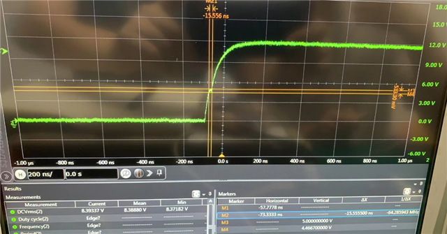
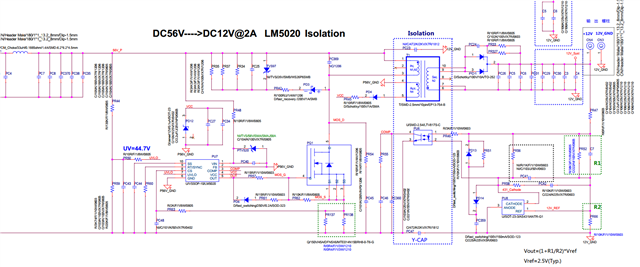
At no load, what should the OUT point of the LM5020-based flyback converter and the waveform between the drain and source of the MOSFET look like?
Is the waveform below normal? (voltage between drain and source of MOSFET)
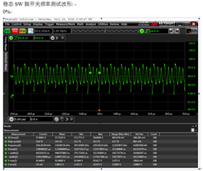
At no load, what should the OUT point of the LM5020-based flyback converter and the waveform between the drain and source of the MOSFET look like?
Is the waveform below normal? (voltage between drain and source of MOSFET)