A related question is a question created from another question. When the related question is created, it will be automatically linked to the original question.
If you have a related question, please click the "Ask a related question" button in the top right corner. The newly created question will be automatically linked to this question.
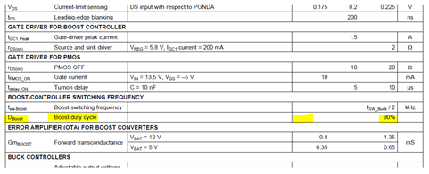
The boost controller allows the device to operate down to 2 V at the input; the duty cycle of Boost converter D = 1 – (input voltage/output voltage); so, it depends on your output voltage selection (7 V, 8.85 V, or 10 V), the minimum possible duty cycle should be: 71%; 77.4% or 80%. The 90% max duty cycle means the input voltage should be > 1/10 of output voltage.
Thanks for the response. design is for Vout=10V, Switching frequency is 255kHz. I wanted to know the minimum duty cycle that the controller can achieve, means What is the minimum difference needed between my input and output to work the controller as a boost?
Eg: If my input is 9.99V and Vout =10V, the calculated D = 0.1%, which means, that the low side switch On time is around 4.03µs and the high side switch-off time is 4.03nS. Whether this condition can achieve? Does it have a limit of minimum DC? if yes, how much it is? When the controller stops switching and bypasses the input as it is a pre-boost? the input range applicable is 8V to 16V.
I hope you understand the question and waiting for your response.
I have the EVM setup for Vout=10V, switching frequency is 200kHz (The closest option on the EVM to 255kHz). I got following test results for you:
The booster works from 8.53V to 10.25V from VBAT power up; it works as a bypass switch beyond the range.
After the booster starts up, it works down to 2V with 200KHz switching frequency .
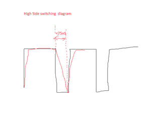
The high side switch-off time keeps at about 75nS after VBAT>9.5V but switching frequency keeps lowering down from 200K down to 72Hz when VABT=10.24V just before it stop switching.
Thank you so much for your testing observation. Can you help me with the following queries?
1.) May I know what this range from 8.53V to 10.25V is? could you be able to see the switching in this range? eg: You could able to see switching at 9.5V, is my understanding correct? what about less than 8.53V?
2. Sorry, I didn't understand the observation, Could you explain?
3. So, my high side switch should be able to switch off time at least 75nS? This implies I should have a MOSFET with a fall time<75nS as my high side drive. Is my understanding correct?
When apply VBAT in the range of 8.53V to 10.25V (which means 8.53V<VBAT<10.25V), the device can power up WITH the booster switching and booster output is 9.95V. When apply VBAT out of the range above (which means either VBAT<8.53V or VBAT>10.25V), the device powers up WITHOUT the booster switching; the booster works as a bypass switch. For example, if VBAT=8.50V, booster doesn't switching and its output is 8.35V (with about 150mV drop); if VBAT=10.50V, booster doesn't switching and its output is 10.35V (with about 150mV drop).
When apply VBAT in the range of 8.53V<VBAT<10.25V, the device can power up WITH the booster switching and booster output is 9.95V. From here, I did monitoring the booster switching and lower the VBAT slowly, the booster stopped switching when VBAT=1.99V.
Yes; please refer to the TPS4333xEVM User Guide for the MOSFETs part number. I found the booster switching waveform on the EVM is not very good ; I suggest to use faster MOSFETs.
Thanks again for your detailed explanation. I'm still confused a bit about #1 and #2. In #1 you said <8.53V there is no switching and bypassing the input voltage with some voltage drop. also in #2, the booster stopped switching when VBAT=1.99V. May I know the behaviour in between?
Also, Any idea, why the booster is not boosting the voltage to less than 8.53V? It's supposed to boost the voltage right?
The device is designed for power supplied from car's 12V battery; its booster is designed for the battery voltage lower than its normal level caused by its engine starting moment. Please see specs below for VIN 2V to 40V with condition of "Boost controller enabled, after satisfying initial start-up condition".
So, VBAT>8.53V is the "start-up condition"; the booster stopped switching when VBAT=1.99V is normal specs.