


Other Parts Discussed in Thread: BUF602,
Dear TI experts,
I'm designing a system using the TPS65133 to power a high speed op amp (BUF602).
In my application, Vi comes from 3.7V from a 350mah Lithium battery.
Currently, I have some problems with layout settings.
1. AVIN and PVIN must be connected together on another layer, will shorting these two PINs directly cause any problems?
2. Is there anything wrong with my component layout connections and ground plane design? Do the pads in the middle of the TPS65133 require heat dissipation?
3. Are thermal vias necessary? Because the manufacturer said that punching holes on the pad may cause problems with soldering. Or should I change the vias to small round through hole pads?
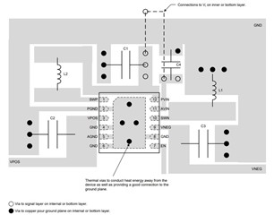
My layout setup is shown below.
Since I have other ICs on the front layer, the TPS65133 and its necessary components are on the bottom layer of the PCB.
The three figures below are the layout I set based on the TPS65133EVM.
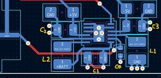
Bottom Layer
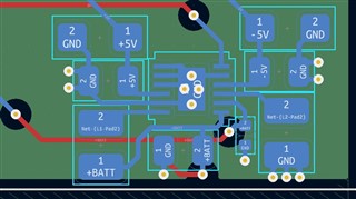
Ground Plane
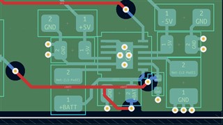
Front Layer
Best regards,
Will

