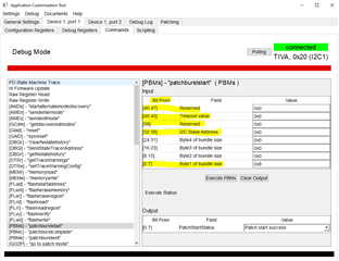
In the TPS6599xAD_TRM_slvubt3.pdf document section 4.7.1 the Input DATA register layout description seems wrong.
It shows Bytes 0-3 as the bundle size, but shows bits 39:32, 31:24, 23:16, and 15:8 which would be Bytes 1-4
It shows Byte 5 as the I2C slave address and Byte 6 as the Timeout value
There is no Byte 4 shown.
Is Byte 0 where the Status is placed on Output, while Bytes 1-6 are used for the Bundle Size, Slave Address, and Timeout on Input?