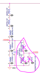
This thread has been locked.

If you have a related question, please click the "Ask a related question" button in the top right corner. The newly created question will be automatically linked to this question.

UCC28064A: Vbulk drop during startup

Part Number: UCC28064A

Hi team,

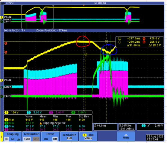
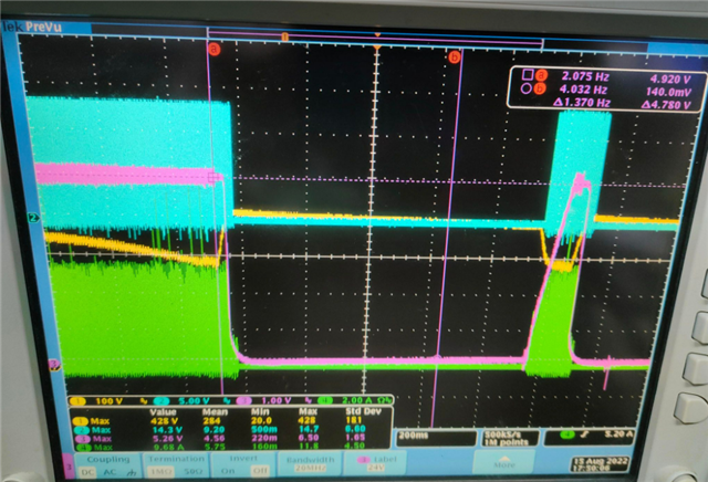
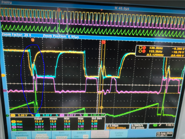
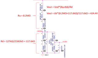
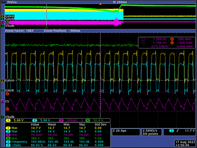
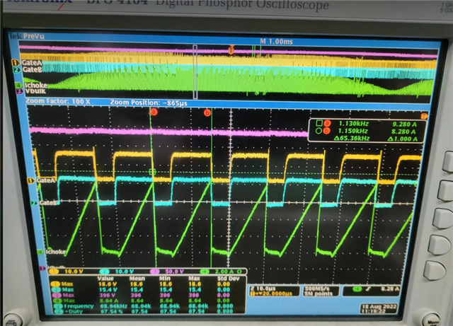
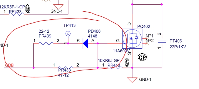
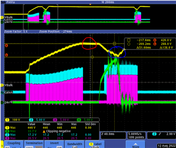
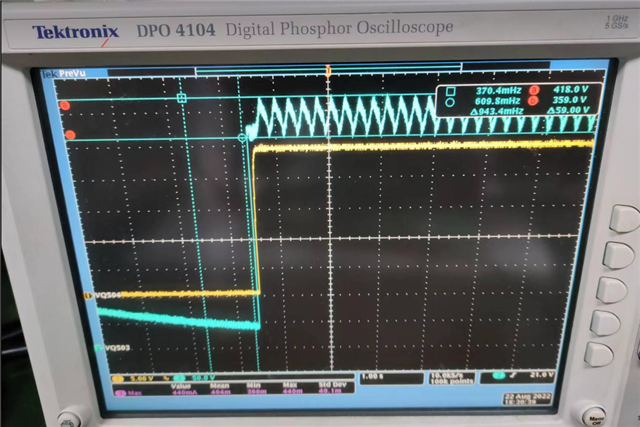
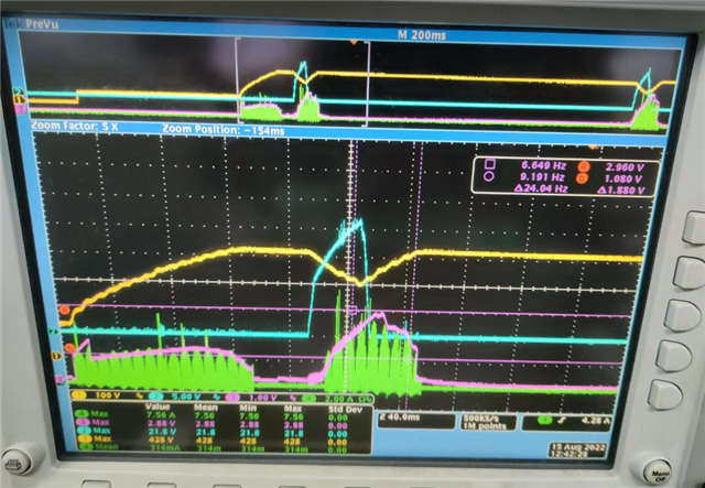
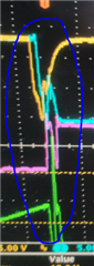
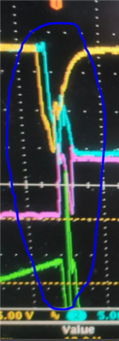
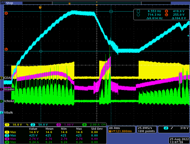
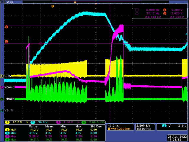
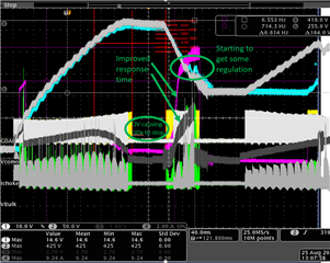
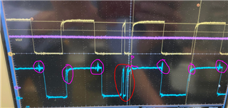
my customer found its PFC output drop to 288V when at higher power load which cause LLC shut down, we suspect this might be OVP since the output reach 426V which is above OVP 422V,

I wonder why this OVP happen if most of the parameters follow calculator tool,

what action can we take to avoid this?

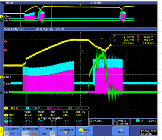
BTW, duty cycle is  95%

below excel is the issue organized by them , please refer to it for more detail.

Interleave 500W PFC issue 20220812.xlsx

  • Hi Fred,

    If this is the same design you shared in the other UCC28064A post, do you still have this connection on VSENSE that we discussed there? If so, please remove the circled components and check operation again:

    If the issue still exists, please share the rest of the schematic with the LLC circuitry and connections.

    Ray

  • Hi Ray,

    I'm curious why we can't do this way ,

    I thought as long as the Vsense and HVsense are at the same exact voltage as the original two independent divided voltage in the calculator then it should be OK,  is there any other potential risk that I miss here  , for example transient?

    here's the four conclusions I discussed with local  AE Adam:

    1. the red circle is the OVP during startup overshoot, Adam recommend remove the Vsense cap PC410 to increase the response, do we also need to remove PC418?

    2. as for blue circle is because of the insufficient transient response, since NXP LLC has UVLO function, so when drop too much the LLC will be turn-off.

    Adam recommend revise compensation network. any feedback on this?

    3. the third case is when customer slowly increase the load, the Vcomp (pink one) reach 5V  when output is 360W, 

    but the maximum load is actually set at 500W, which means Vcomp is unexpected higher .

    any idea why and how we can fix this?

    4.  this is also quite serious ,  they found unexpected peak current (green) and GDA GBB pulse at same time (yellow & blue) , which is abnormal.

    Adam suggest increasing the RC filter at CS pin, let me know if think different, thanks


    please help on above four comments, customer's quite confused right now, thanks

    Regards,

    Fred

  • Hi Fred,

    Ray is out of office. He will be back by tomorrow. So, he should be able to respond you back within 2 days.

    Regards

    Manikanta P

  • Hi Manikanta,

    this case is in urgent . is there any chance I could get a response today?

  • Ray is the one who knows this part very well. You should wait atleast a day to get the response.

    Regards

    Manikanta P

  • Hi Fred,

    In regards to the HVSEN connection, the general idea is to have two independent over-voltage sense paths, one from Vout to VSENSE and the other Vout to HVSEN. The way it's configured now, the HVSEN threshold is VERY low so it will never see 4.67V.

    1. If this is the same design you shared in the other UCC28064A post, I calculate the parallel resistance from VSENSE to GND (Rd) to be 117.56kΩ. This would result in a regulated output of ~424V which is exactly where the output appears to be going in your first scope capture. So it doesn't appear to be OV, simply voltage regulation with the chosen values.

    2. I think it is wise to increase the compensation. Try increasing PF430 by 2x up to 4x (12kΩ up to 48kΩ) to improve the response.

    3. This means the design isn't designed correctly for 500W. Reduce the current sense resistor(s) proportional to the difference you are seeing (~ 40%)

    4. It appears that the MOSFET is being triggered to turn on just after being switched off and you are getting reverse recovery. This is likely due to the ZCD signal bouncing around. Try increasing PR401 & {R433 by 2x - 4x to see if this corrects the issue. You can probe ZCDx along with the above waveform first to confirm and then increase the resistor until the condition is resolved. You can then fine-tune the R-C to get the delay you need on ZDCx.

    Regards,

    Ray

  • Hi Ray,

    thanks a lot for your feedback.

    1. I'm really sorry, I didn't update the latest value since they had changed it,

    PR448+PR424=150K

    PR427=390K

    PR449=470K,  which will give you about 392V Vout as you can calculate yourself.

    150K || (390K+470)=127K

    6Vx(8.2M+127K)/127K=392V, so it should be ok

    how about the feedback on PC410 and PC418 to prevent large overshoot?

    3.

    would you explain why  decreasing the Rsense would help?

    I thought that was only for OCP. Vcomp should be related to Vinac or Rset?

    and do you think the issue four could be the root cause of this?

    4. 

    I understand the drop of ZCD may be due to resonant recovery in DCM, but it could also caused by OCP.


    do the GDA and GDB in this picture looks OCP to you since they both turn off and turn on at same time.

     we still suspect that there might be a risk that CS pin ( pink one in this picture) is coupling and being triggered  even though the cs pin in this picture has not reached  -0.2V yet... but we don't know the real CS signal

    let me know your feedback?

    BTW,  the pink signal in the previous picture is ZCD, in case you didn't know.

  • Hi Fred,

    1a. Your updated values make sense for 392V. However, HVSEN = VSENSE * 470/(390+470) = 0.547VSENSE. When VSENSE hits HIGH_OV at 6.67V, HVSEN = 0.547*6.67 = 3.68V which is still below 4.87V HVSEN_OV threshold.

    1b. Removing PC410 and PC418 should improve the response (but may leave it vulnerable to noise). I think increasing PR430 as suggested is important to speed up the response time.

    3. My suspicion is that it is going into current limit before reaching the desired maximum power level

    4. The GDx signals will operate in phase when OCP is hit. This does appear to be a case of OCP being tripped on every cycle. CS is bandwidth limited, so it's not easy to say if it's crossing 200mV. You can try to improve the filtering on CS (as Adam mentioned), but I would also lower the RSENSE value.

    If things still don't work as expected, it would be helpful to see the inductor current.

    In the future when you share waveforms, please also indicate the power level (or output current) and Vcomp value

    Regards,

    Ray

  • Hi Ray,

    1 a. OK thanks, but HVSEN_OV is supposed to be  higher bar than  HIGH_OV, so I think it's  not the root cause, but yes I'll tell them to increase closer to 4.87V 

    1 b, they said the GDA pin was damaged right after they change PR430 to 20K., which is weird, is this possible?

    3. so the Vcomp will be 5V during OCP event , correct?

    4. the previous picture was 24V/15A, you can see the drop at output,

    after they reduce the Rsense from 0.01 to 0.005 ,  the PFC now can reach 500W(24V/21A shown below)  without any drop.

    however, there's still a in-phase issue there (yellow and blue) which is OCP sign,

    should we keep reducing the Rsense ? or is there any other potential  risk ?

    Regards,

    Fred

  • 1a. That sounds more reasonable to adjust the value so that it is possible to utilize both HVSEN_OV and HIGH_OV. I'm still not sure why it was connected this way as it complicates things and results in an extra cap across VSENSE.

    1b. That doesn't make sense that GDA is damaged, especially with this change. It's more likely the gate of the MOSFET is damaged (preventing GDA from switching). Still, the change wouldn't do this unless it resulted in a an unstable current signal.

    3. During OCP, you won't reach your desired output so the error amp will drive Vcomp up to the limit.

    4. Good to hear they are now achieving the full power level. 0.005Ω would indicate ~0.166V/0.005Ω = 33A of peak current which seems high for this design. Can you confirm the current is getting this high?

    Ray

  • 1a. I understand your confusion, the reason they do this is because they have to pass ERP lot 5 which very care about super light load efficiency, so we need to integrate two divide resister to pass the power consumption. 

    1b. maybe change PR430 to 20K make phase margin too low so oscillate.... I tell them to try lower..

    3. got it,  since if both DRV are in-phase we can deliver to maximum power normally , right?

    4. yes,  the E-load sink total 500W during 24V output, but the current shown in the green signal in the picture looks normal,

    I think maybe cs pin is coupled or some unknown interference, I'll send you the layout for you to check tomorrow.

    how about just short the Rsense to check if this help? or it's too dangerous?

    thanks for your help

    Fred

  • Hi Fred,

    Regarding #4 : I'm not sure what the FET current rating is, but a more prudent step would be to lower Rsense a little more. The current through Rsense is shared between the two output stages, so you may be OK to lower it further.

    You can short out Rsense but the risk is damaging the MOSFETs. If you can tolerate potentially damaging the components on one board, it may help with this debug if lowering Rsense some more doesn't get you closer to a solution.

    Is PC406 right next to the CS pin on the UCC28064A?  You can try to reduce it down to 1nF

    Ray

  • Hi Ray,

    1b. would you check what's wrong in the schematic or layout regarding why the GDx pin so easy to be damaged?

    I suspect may be parasitic ringing?

    2. do you know why there's OVP(red circle) during soft start? I know there should be overshoot  during soft start,

    but why does it just go all the way up instead of settling to 390V

    4. I thought we should increase the RC filter on this to filter out the high freq noise on CS instead,

    would you explain why you want to reduce it?

    Layout.brd

    I've upload the layout, there's so much weird thing that can't explain , would you check layout if there's something weird, for example why there's always OCP at CS pin

  • Hi Fred, please give me until Monday to respond.

    Ray

  • Hi  Ray

    sure, I understand layout review take some time

  • Hi  Ray,

    how's layout reviewing?

    adding one question, please also answer previous question along with this one

    they discover this issue only at "264Vac" during loading above 4A,

    does this has something to do with the compensation or ZCD current not enough?

    Regards,

    Fred

  • Hi Fred.

    This is another new issue that's being added to this thread. There appear to be a lot of "moving parts" on the test and debug of this design. I think we need to isolate the PFC from the LLC. Essentially, we need to debug only the PFC portion of the design.

    Please disconnect the PFC from the downstream circuitry and apply the load directly to the Vbulk output. If you don't have access to a high-voltage electronic load, then use a resistive load.

    After that, please summarize the issues that still exist.

    Thank you,

    Ray

  • Hi Ray,

    the above issue is probably due to ZCD threshold too low , I know the root cause now.

    but could you please still answer the previous questions four days ago ? we still need those answers from you to rule out some causes. 

    and we have been waiting for four extra days just for your layout review, could you at least give comment on layout , especially Current sense?

    I don't think LLC is the problem to all these since if the output is stable 390V, LLC should be OK.

    but as we know there're still a lot of problem is happening during steady state. so I don't think customer would buy in  unless we give them enough reason.

  • Hi Fred,

    Regarding your questions:

    • I don't know why the output is going OV after startup. The only explanation that I can think of is that the loop is extremely slow to respond. The values in the schematic seem reasonable, but I wonder if the values populated on the board are different (perhaps due to a build error). Verify the compensation values with an LCR meter.
    • I don't see anything wrong with the gate drive circuitry. Perhaps you can put a probe on GDA and inspect the signal.
    • The switching frequency is 100kHz or 10uS/cycle. PC406 at 1uF and PR410 of 100Ω results in a 100us time constant. Lowering it to 1nF will result in a time constant of 100ns. You want the CS circuitry to be able to react quickly to the voltage across Rs. 100Ω/1nF is recommended on this pin. Also, I recommend verifying that PC411 is unpopulated as indicated in the schematic.
    • I looked at the CS signal layout and I don't see anything specific that would result this issue.

     I have a few questions:

    • Are you working on this board in the lab or is it the customer? If it's the customer, I would understand the resistance to removing the LLC. However, if you are convinced the LLC is fine, then it would make debug more straightforward by isolating the PFC circuit block from the rest of the board. It seems easy to do by removing a couple of the jumpers on the board.
    • Did you confirm that it is the GDA pin that is damaged and not the MOSFET?
    • Can you confirm the current is reaching 33A peak? (by capturing the current waveforms)
    • Did you lower Rsense further than 0.005? If so, by how much and what was the result.
    • Did you lower PC406 to 1nF?
    • Please summarize the state of the design as I'm not quite sure which issues have been resolved and which ones still remain.

     If you've verified the compensation components and still have the startup OV issue:

    • Please add Vcomp to the captured waveform. You can remove GDB to free up a channel
    • In the captured waveforms, please reference signals (voltage and time) to the major gridlines so I can make more accurate measurements from the waveforms.

    Ray

  • Hi Ray,

    the board was in customer's lab, fortunately it's sending to TI's lab now.

    • they said they increase the Rcomp to 20K but no improvement on the drop ( blue circle)

    answer:

    • GDA's damage since they change IC and can get back on
    • like I said before, they can operate at 500W after change to 0.005 ohm, but two phases is still in phase (OCP). I mean it would drop at 500W before the change.

    for startup OVP, please see below,

    Vcomp is not 5V, so no OCP during startup scenario I suppose,

    maybe overshoot is too large and it reached 428V and stuck at OVP and Vcomp discharge until the voltage drop during LLC voltage rise up

    pink is the Vcomp, yellow is PFC output, blue is LLC output, green is current

    moreover, we organize all the issue so far , you can see it as the version without any changes in the beginning.

    please help check

    1581.Copy of Interleave 500W PFC issue Summary 20220824.xlsx

  • Hi Fred,

    The waveform really helps. I can clearly see that the loop response is too slow. I recommend you re-try the experiment of increasing PR430 to speed up the response. I recommend you install a 27kΩ and re-collect the same waveform.

    Regarding the CS pin layout, I do see an improvement that would likely help. This is something you can try on the existing board (perhaps using an 0805 or 1206 cap to bridge over the (unnecessarily) wide trace going to BRST. As you can see, the ground going to PC406 can be made much shorter. Additionally, it is currently running along-side GDB which is noisy.  This is my suggestion for a new layout:

    If you can make mimic this change on the existing board, replicate this earlier scope capture to see if the noise on CS is reduced or eliminated. Also, if noise is coupling in from GDB, a larger cap will make this worse, not better.

    There are other suggestions on the layout, but I want to focus on what's causing these current issues where you are unable to regulate.

    Regards,

    Ray

  • Hi Ray ,

    really thanks a lot for your help,

    I will let customer know your suggestion

    • would you explain more on why larger cap won't help this coupling from GDB?x
    • and I'm not sure what's your comment on this picture, since I can't match the previous context with this 

  • Hi Fred,

    I'll share with you my thinking regarding the issues with this board so you can have more insight into my observations and questions...

    I believe there are at least two issues you are fighting. There may be more, but until we get past these two issues, it'll be difficult to distinguish other issues:

    1. Slow voltage loop response causing the issue demonstrated with the scope capture (with Vcomp) that resulted in OV, re-start, OV, etc...

    2. Noise on the CS pin causing the MOSFETs to turn on when they should not be. This will result in unpredictable behavior and can damage components on the board.

    For #1, by increasing Rz (PR430), you actually speed up the response of the loop, not slow it down. Vcomp will rise faster and it will respond more crisply to VSENSE and if set properly, will not result in erroneous OV. Regarding the damage to GDA that the customer reported as a result of increasing this resistor, I can't think of any reason that doing this would damage GDA. However, I recommend having a scope connected the first time you power up after this change so that if damage does occur, it is captured and we can analyze.

    For #2, I was initially thinking it had to do with the ZCDx signals bouncing around. After reviewing all of the waveforms, it looks like something else is causing the MOSFETs to turn on suddenly, resulting current spikes. The pulses are so fast (as shown in the circled image above), that it appears to be induced noise. I'm not positive that the CS filtering is the source of the noise, but If the noise is being picked up by the area of the board that includes the CS capacitor and it's path to ground, then by making the capacitor larger will only increase the noise coupling.  By adjusting the capacitor and it's path to GND, you can demonstrate (or eliminate) this as the cause of noise cross-coupling between CS and GDB. 

    I hope this helps.

    Ray

  • Hi Ray,

    thanks for your reply again.

    • like you suggested, they bypass the PC406 ground directly to the IC, but the drop is still there during startup.

    but I think this one is  more related to the in-phase issue instead of start up issue, so I'll ask them to check the GDx in-phase during 400W~500W.

    agree?

    • after that they changed the Rz to 27K, you can see the drop is still there and Vcomp has increase prominently to 5V.

    and like I said before the GDB is damaged again after they change to 27K  for a while.

    I can see the Vcomp is high enough which means Ton is high enough but still drop, could this means the LLC startup sink unexpected current that PFC can't afford?  BTW, they use NXP LLC

  • Hi Ray, 

    any update?

  • Thank you for making the changes. 

    Yes, the issue I'm trying to solve with the CS cap is related to the in-phase issue and false triggering of phase B. As far as the actual modification, the picture is not clear, but it looks like the cap was moved to the AGND pad and wired back to CS. If that is what they did, I would ask that they shorten the wire from the cap to the device pin. A short bus wire would be better:

    Regarding the startup into OV, we've made some progress by getting COMP to respond more quickly; it's not perfect, but better. It looks like you now need to increase the on time to get even more power available, especially for when the LLC turns on. You also may end up needing more output capacitance, but I think the first thing to try is to increase the on time. You can do that by lowering Rset. If you start by lowering by 25%, so from 165kΩ to 124k. This will increase the average current proportionally. I don't know what the MOSFET or inductor ratings are, so you may have to adjust Rsense to protect them.

    What is your inductor value and current ratings? What MOSFETs are you using?

    Please share similar waveforms after you've made a change to Rtset.

    Thank you,

    Ray

  • Hi  Ray,

    thanks a lot,

    • yes, the CP406 is vertical soldered like you saw, I tell them to check, but I think this modification is still better than before

    • the inductor now is 140uH,    I see your point now trying to be faster and faster. since Ton would increase with Vcomp theoretically,  so it  is supposed  to show some improvement at least , and you can see  we did give input current to LLC (green signal) than before, but as we can see , the drop still there and clear .     don't you think it's strange that there's not a single improvement after we increase Rz so much.
    • BTW, Ray , one question ,  base on the previous start up picture (before change to 27K),  the Vcomp didn't reach 5V at all, does this mean there's no OCP possibility at all and so we can rule out this factor?  

    since if it's OCP, the Vcomp is supposed to be 5V, right? please correct me if I'm wrong

    update MOS specTSM60NC165CI_A2104+(update).pdf

  • Hi Fred,

    As far as the modification, I don't have an issue with where the cap is placed. There were two reasons for the change:1. to move the CS filter path away from noisy GDB and 2. reduce the filter path length. What they did resolves the first issue (though being a large loop, it's they've formed an antenna which may pick up noise). Shortening the wire will resolve the second issue.

    I don't think OC is occurring, otherwise, the gate signals would stop. In this case, they are clearly shutting down due to OV.

    The improvement is definitely there. You can see the improved response time to the load step:

    COMP is now able to demand full power quickly enough. We just need to increase the power that's available by increasing the on time.

    Ray

  • Hi Ray,

    thanks your explanation,

    • they want to reduce the Rset as well,

    but like I said they damaged the GDx so easily under faster response for unknown reason,

    due to the limited numbers of samples and board, they're afraid to continue until we can solve this damage issue,

    I knew you said you're not sure why either,

    but just want to know could we solve this by adding diode to clamp the negative voltage (anode at GDx)?

    since this is highly possible due to  the negative ringing voltage over the absolute spec.

    • one question unrelated to startup,  will Vcomp reach 5V when OCP whether is caused by over-load or coupling on CS pin?

  • A diode clamp at each of the GDx pins can be used to clamp any transient voltages. A Schottky is recommended for its low Vf. It would need to be right at the device pin to be effective.

    Vcomp can reach 5V even when OCP is triggered, it is completely dependent on the signal from the error amplifier.

    I would like to reiterate my suggestion of lowering PC406 to at least 10nF (and PR410 =100Ω) so that the CS block can react quickly enough to protect the MOSFETs. Now that we're increasing the on-time, this protection is more important.

    Ray

  • Hi Ray,

    • update news,

    after Adam and I move the resistor (PR410) of CS RC filter close to IC shown below,

    the OCP in-phase problem is solved. seems like the original jumper is coupled with noise.

    we'll moving on startup problem, and about this we'll ask customer to increase the soft start time,

    since it might be the reason why we have to increase so much compensation and on-time to catch up, which will end up totally different from excel calculator,

    do you think this is due to LLC soft start sinking current too much?

    • another question here, below is the original OCP behavior before update,

    would this in-phase pulse cause hard switching and consequently cause large negative voltage?

    since Adam and I think this might be the reason cause GDx damage so easily . as you can see the measurement , the GDB even reach -4.2V...

    please let me know why this would cause negative voltage if you also agree

  • Hi Fred,

    This is great progress. Good work! This appeared to solve the major problem of noise coupling into CS

    Regarding increasing soft-start time, yes, that will allow time for the PFC output to deliver the required power. If this doesn't resolve the issue completely, you may still need to increase the on-time and/or the PFC output capacitance.

    As you observed, these pulses are creating a negative spike when the falling edges occur simultaneously. I don't see why the scope reports -4.2V, but I can see at least -1.5V (but for a very short time). Certainly if this is repeated many times or is more pronounced, it could cause component damage.

    Regards,

    Ray

  • Hi Ray,

    I've tried to increase Rcomp to 20K tomorrow and decrease Rtest to 124k ,  power on without any load.

    unfortunately , like customer said. the GDx is damaged, seems like so is VCC.

    we can't continue the solution we planned until we can fix this issue first,

    Adam said it's due to the grounding loop is too long causing inductance and negative voltage during turning off rapidly ,

    but I just don't understand why this change will cause turning off rapidly. why it won't happen with original compensation?

    and for the picture we discussed yesterday,

    why would GDx be affected to negative when OCP trigger? 

    if the answer is the same as above , you can answer both at once

    ,and would be better if it comes with a solution.

    thanks


  • Now I see the big negative spike (-4.2V), it's right on the zero time axis (it was hiding on the line).

    I don't think it's OCP causing GDx to be affected. Those spikes are likely due to stray inductance(s) in the GDx path as well as GND. GDB is particularly long which makes it more susceptible.

    Do you know where this noise is coming from? Are they still present with the changes to the CS filtering?

    It's showing up in GDB and I wonder where else it may be. It's almost, but not quite, synchronous with the gate drive pulses. I looked closely and it's not GDA feeding into GDB (or the other way around), so it's coming from somewhere else. Almost a beat frequency component. From the LLC?

    Ray

  • Hi Ray,

    would you elaborate why we focus  on the ground loop of MOSFET ( base on your picture) ?

    GDx is coming from VCC source,

    I thought we should refer to the VCC ground loop instead of MOS ground loop, please correct me if I'm wrong. thanks

    I need to know the detail of root cause to decide the  schottky diode location?  anode and cathode ,respectively.

  • Hi Fred,

    Sorry for the confusion. The reason I highlighted the power ground was in reference to the noise pulses I circled.

    Yes, for the GDx going negative, the ground loop that you highlighted is a good candidate to correct the issue.

    You can try adding a 1uF cap close to the pin and that may prevent much of the negative overshoot. If this doesn't work, this is where you would put a >15V Schottky for protection (cathode on GND, anode on GDx). However, with proper layout, this would not be required.

    Next board, I recommend they follow the layout recommendations: https://www.ti.com/lit/pdf/slua959

    Ray

  • Hi  Ray,

    thanks, extra cap is good idea.

    but I thought it should be another way around, right?

    I mean cathode on GDx and anode on GND, since now GDx is the one show negative.

    Vf of our schotty diode is 0.5V, with above setting so we can make sure the GDx pin voltage doesn't go below -0.5V.

    please correct me if I'm wrong.

  • You are absolutely correct Fred. Sorry about that. Just so we're clear...