Other Parts Discussed in Thread: UCC27518
Dear TI experts,
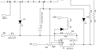
The following is the circuit on our new product, please help to review whether there is any problem with the design, thank you!

This thread has been locked.
If you have a related question, please click the "Ask a related question" button in the top right corner. The newly created question will be automatically linked to this question.
Hi Rogers,
Thanks for reaching out on E2E!
Please see the following feedback:
IN: Input looks good. If there is a lot of noise on your input waveforms, consider adding an RC filter with a TC of no greater than 20 ns.
EN: I notice that the label is a NC there on the schematic provided, but I am assuming it is enable. As seen in the schematic, if you would like to keep the device always enabled, keep it pulled high to VDD.
VDD: For the VDD bypass capacitors, a 0.1-μF ceramic capacitor should be located as close as possible to the VDD pin of the gate driver. In addition, a larger capacitor (such as 1 μF) with relatively low ESR should be connected in parallel and in close proximity.
GND: Looks good.
OUT: I am under the assumption that you are paralleling FETs on the output. If this is the case please be aware that as the number of FETs increase, the gate capacitance increases which leads to an increase in turn on and turn off times of the FETs.
I will also attach a schematic review template for the UCC27518/9 devices to further supplement.
UCC27518_9 Schematic Review Template (1).xlsx
I hope this helps!
Thank you,
Kevin