This thread has been locked.

If you have a related question, please click the "Ask a related question" button in the top right corner. The newly created question will be automatically linked to this question.

UCC27211: Output does not follow input

Part Number: UCC27211

Hi all,

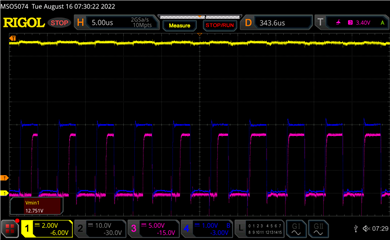
As the title suggests, the output of the low-side gate driver does not follow the input correctly as you can see in the picture below.
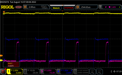
  • CH1: Supply voltage
  • CH3: Output of gate driver (LO pin)
  • CH4: PWM input (LI pin)

The gate-driver does turn of at the correct moment but the turn-on is significantly delayed which leads to shorter pulses.
There are 4 drivers in the circuit, each showing the same problem.

What is also strange is that the driver starts to operate normally after 100µs (see next picture).
Some additional information which might be help to find the problem:

  • The supply decoupling capacitance is 4.7µF (and I don't think this is the problem since the supply is not dropping below the UVLO)
  • Gate resistor is 10R and the MOSFETs gate capacitance is around 3nF
  • Switch node voltage is 30V
  • LI and HI have 1nF of decoupling capacitance directly at the input pins of the driver

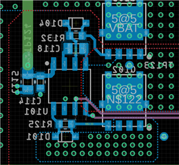
Below you can see the PCB layout:

Any help is highly appreciated.
Thanks in advance.

  • Hello Markus,

    Thank you for the information on your application. I have a question on the plots. On the plots shown, is the high side switching along with the switch node when you show the unexpected LO turn on delays? Most of the layout looks good regarding the routing and placement of VDD and HB capacitors. I do have one comment, it looks like the switch node (plane) may be very close to the driver input pins. 

    Are the scope plots and behavior during when the board is going thru startup? Or can you confirm the operating condition where you see the questionable behavior. 

    Can you confirm the following: 1) with no high voltage applied to the Mosfets, does the LO and HO timing look correct? 2) since the switch node is close to the driver input, can you add a 50 ohm resistance and 100pF on the driver inputs, with the capacitor placed close to the IC pins and confirm if there is any improvement?

    Can you provide plots of the questionable behavior and also show the switch node trace and HO trace?

    Regards,

  • Hello Richard,

    I did some additional measurements including the switch node and the HO signal.

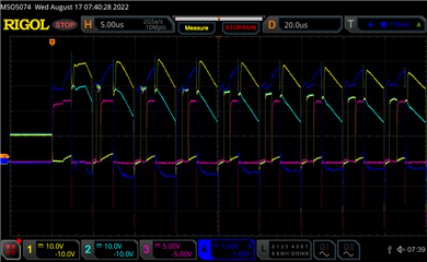
    Startup

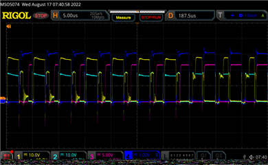
    Transition to normal behaviour

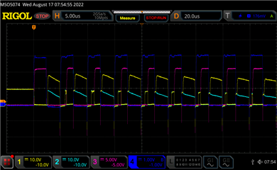
    Without high-voltage applied

    • CH1: HO Signal
    • CH2: SW node
    • CH3: LO Signal
    • CH4: LI Signal

    Measurements have been taken without a GND spring so the negative voltage spikes might not be as high as it seems.

    Regarding your questions:

    • The driver input signals are indeed close to the switch node but they are on the inner layer of the PCB with a GND plane between the SW node and the signals
    • This behaviour can be only encountered during startup, as you can see in the plots, the driver start to work normally after around 200µs.
    • Without the high-voltage applied to the MOSFETs, the problem still exists but it only takes ~50µs until the driver resumes normal operation
    • Unfortunately since the driver input signal are on the inner layer of the PCB, i can't botch in the resistor but I did solder 1nF directly to the pins of the driver but this did not help.
    • As I mentioned earlier, the negative voltage spikes might be not as bad when measured with the GND spring but they are definitely there, could this be the problem? The datasheet mentions that the driver es quite tolerant to voltage transients so I would assume that this should not be root cause.

    Thank you very much for your help!

  • Hello Markus,

    I have some questions on the plots. In the 1st plot I see an unexpected and unusual waveshape on the LI input with the signal going below ground and unexpected rising slopes when it looks like LI should be high. On the second plot it looks like LI is closer to an expected square wave shape referenced to ground. Do you know the cause of the LI waveform during startup? Is there resistance between the controller ground and ground reference of the driver?

    Also on the HO and HS waveforms when HO is high it looks like it follows HS with a DC offset which is expected. But after HO turn off it looks like HO and HS rise high again (same amplitude) for a time. Is that expected in the power train?

    I am curious if you have tested more than one board, and driver device. If not. can you try a different driver device to confirm if the behavior is improved?

    I am also curious to confirm, if the HO output is following the HI input. Can you confirm if this is the case and include plots showing HI, HO, switch node, and LO?

    Regards.

  • Hi Richard,

    We found out that we have very high currents in each half-bridge which was the reason for the disturbance in the measured signals.
    The parasitic inductance also lead to negative voltage spikes when the high-side or low-side switch turns off.
    By increasing the turn-off resistor, we were able to reduce these negative spikes and this did indeed fix the problem.

    So despite the datasheet suggesting that this gate driver uses a very robust design and can handle negative voltage transients, one should take care (either by layout or by increasing turn-on/off resistors) to avoid voltage transients at the input signals.

    This issue is now resolved, thank you for your time Richard!